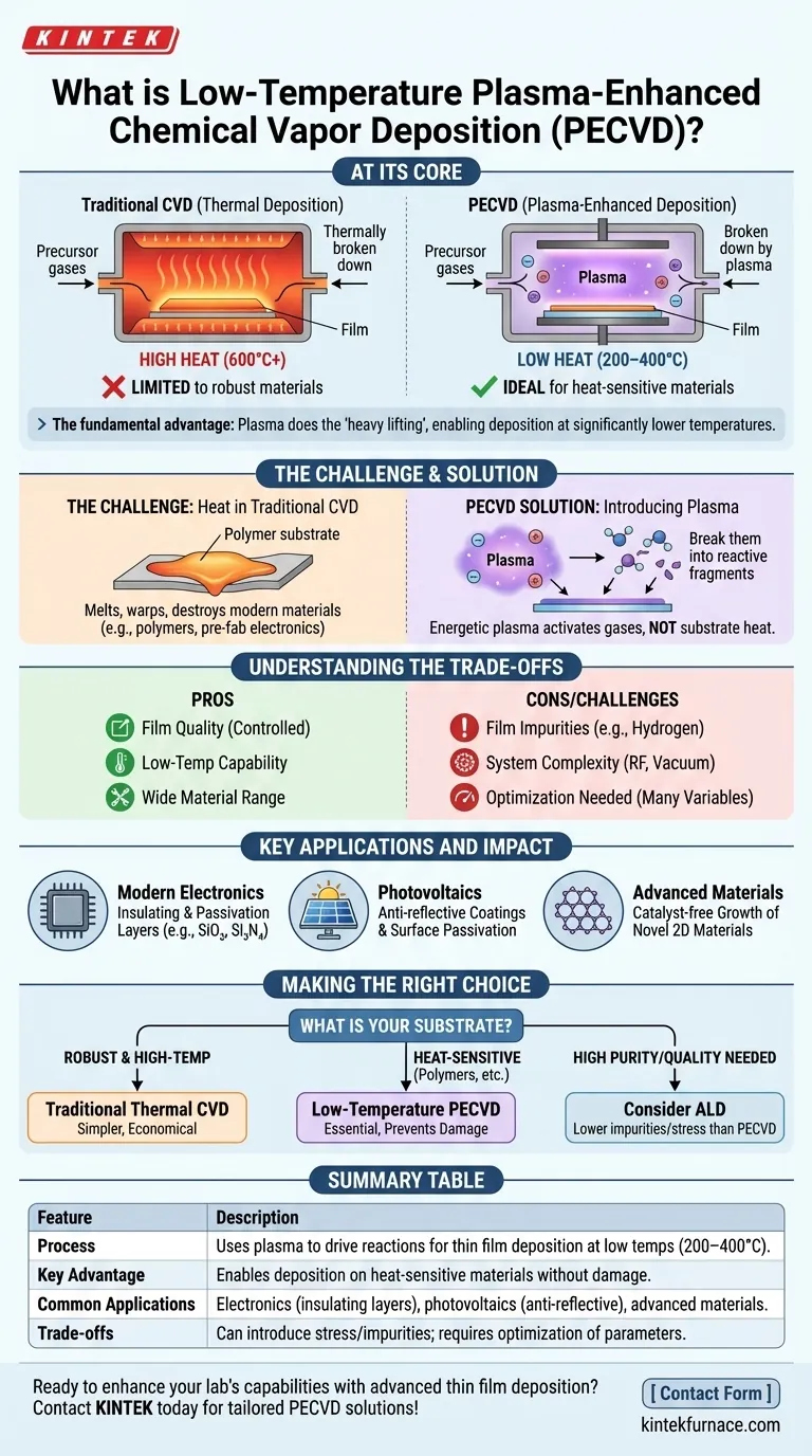
At its core, low-temperature plasma-enhanced chemical vapor deposition (PECVD) is a sophisticated process for depositing exceptionally thin films onto a surface. Unlike traditional methods that rely on intense heat, PECVD uses an energized gas, or plasma, to drive the chemical reactions needed to form the film. This critical difference allows for high-quality deposition at significantly lower temperatures, making it indispensable for manufacturing on heat-sensitive materials.
The fundamental advantage of PECVD is its use of plasma to do the "heavy lifting" of breaking down chemical precursors. This allows deposition to occur at significantly lower temperatures, opening a range of applications on sensitive materials that would be damaged by conventional high-heat methods.
The Challenge: Heat in Traditional Deposition
To understand the value of PECVD, one must first understand the limitations of its predecessor, conventional Chemical Vapor Deposition (CVD).
The Conventional CVD Approach
Traditional CVD is analogous to baking. A substrate (the surface to be coated) is placed in a high-temperature chamber, and precursor gases are introduced. The intense heat provides the thermal energy needed to break down these gases and cause them to react on the substrate's surface, slowly building a solid, thin film.
The Limitation of High Temperatures
This reliance on heat is a major constraint. Many modern materials, such as polymers, plastics, or complex semiconductor devices with pre-existing components, cannot withstand the high temperatures required for thermal CVD. The heat would cause them to melt, warp, or become functionally destroyed.
How PECVD Solves the Temperature Problem
PECVD revolutionizes this process by substituting most of the required thermal energy with plasma energy.
Introducing Plasma: The Key Innovation
Plasma is often called the fourth state of matter. It is a gas that has been energized—typically by a radio frequency (RF) or microwave field—to the point where its atoms are broken apart into a highly reactive soup of ions, electrons, and free radicals.
Instead of slowly baking the materials, PECVD uses this energized plasma to instantly activate them. The energetic electrons within the plasma collide with the stable precursor gas molecules, shattering them into reactive fragments.
The Mechanism of Plasma Activation
These newly created reactive species are chemically unstable and eager to bond. They readily deposit onto the substrate surface, which is kept at a much lower temperature (typically 200–400°C), and form the desired thin film.
The plasma provides the activation energy for the reaction, not the heat from the substrate. This is the central principle that enables "low-temperature" deposition.
Understanding the Trade-offs
While powerful, PECVD is not a universal solution. It introduces its own set of technical considerations.
Film Quality and Purity
The energetic plasma bombardment can sometimes incorporate other elements (like hydrogen from precursor gases) into the film or induce internal stress. Controlling plasma power, gas chemistry, and pressure is critical to achieving a film with the desired density, purity, and mechanical properties.
Equipment and Process Complexity
A PECVD system is inherently more complex than a thermal CVD furnace. It requires sophisticated hardware for generating and containing the plasma, including RF generators, vacuum pumps, and intricate gas delivery systems.
The Need for Optimization
Achieving a specific film property is not trivial. It requires careful optimization of numerous variables, including gas flow rates, pressure, plasma power, frequency, and substrate temperature. This process can be more complex than tuning a simpler thermal process.
Key Applications and Impact
PECVD's ability to coat sensitive materials has made it a cornerstone technology in several high-tech industries.
Modern Electronics
It is used to deposit crucial insulating and passivation layers (like silicon dioxide and silicon nitride) on microchips after sensitive transistors have already been fabricated.
Photovoltaics
In solar cell manufacturing, PECVD is used to apply anti-reflective coatings and surface passivation layers, which directly increases the efficiency of the cell.
Advanced Materials
The technique enables the catalyst-free growth of novel 2D materials, simplifying production and reducing potential sources of contamination for next-generation devices.
Making the Right Choice for Your Goal
Selecting a deposition technique depends entirely on your substrate material and desired film properties.
- If your primary focus is cost-effective deposition on robust, high-temperature substrates: Traditional thermal CVD may be a simpler and more economical solution.
- If your primary focus is coating temperature-sensitive materials like polymers or pre-fabricated electronics: Low-temperature PECVD is the essential and often only viable choice to prevent substrate damage.
- If your primary focus is achieving the highest possible film purity and crystalline quality: You must weigh PECVD against other methods like Atomic Layer Deposition (ALD), as the plasma can introduce impurities or stress.
Ultimately, mastering PECVD is about leveraging its unique ability to decouple the reaction energy from heat, enabling the creation of advanced materials that would otherwise be impossible to fabricate.
Summary Table:
| Feature | Description |
|---|---|
| Process | Uses plasma to drive chemical reactions for thin film deposition at low temperatures (200–400°C). |
| Key Advantage | Enables deposition on heat-sensitive materials without damage, unlike traditional high-heat methods. |
| Common Applications | Electronics (insulating layers), photovoltaics (anti-reflective coatings), advanced materials (2D growth). |
| Trade-offs | Can introduce film stress or impurities; requires optimization of plasma power, gas chemistry, and pressure. |
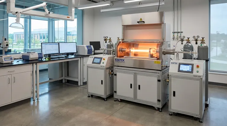
Ready to enhance your lab's capabilities with advanced thin film deposition? At KINTEK, we specialize in high-temperature furnace solutions, including CVD/PECVD Systems, backed by exceptional R&D and in-house manufacturing. Our deep customization ensures we meet your unique experimental needs, whether you're working with sensitive materials in electronics, photovoltaics, or advanced materials. Contact us today to discuss how our tailored PECVD solutions can drive your innovations forward!
Visual Guide
Related Products
- Inclined Rotary Plasma Enhanced Chemical Deposition PECVD Tube Furnace Machine
- Inclined Rotary Plasma Enhanced Chemical Deposition PECVD Tube Furnace Machine
- RF PECVD System Radio Frequency Plasma Enhanced Chemical Vapor Deposition
- Slide PECVD Tube Furnace with Liquid Gasifier PECVD Machine
People Also Ask
- What are the typical conditions for plasma-enhanced CVD processes? Achieve Low-Temperature Thin Film Deposition
- How is heat transferred to the furnace tubes in a rotary tube furnace? Master Uniform Heating for Your Materials
- How does the amount of material processed vary between batch and continuous rotary tube furnaces? Scale Your Production Efficiently
- What are the main advantages of PECVD tube furnaces compared to CVD tube furnaces? Lower Temp, Faster Deposition, and More
- What materials are rotary tube furnaces typically constructed from? Choose the Right Tube for Your Process


