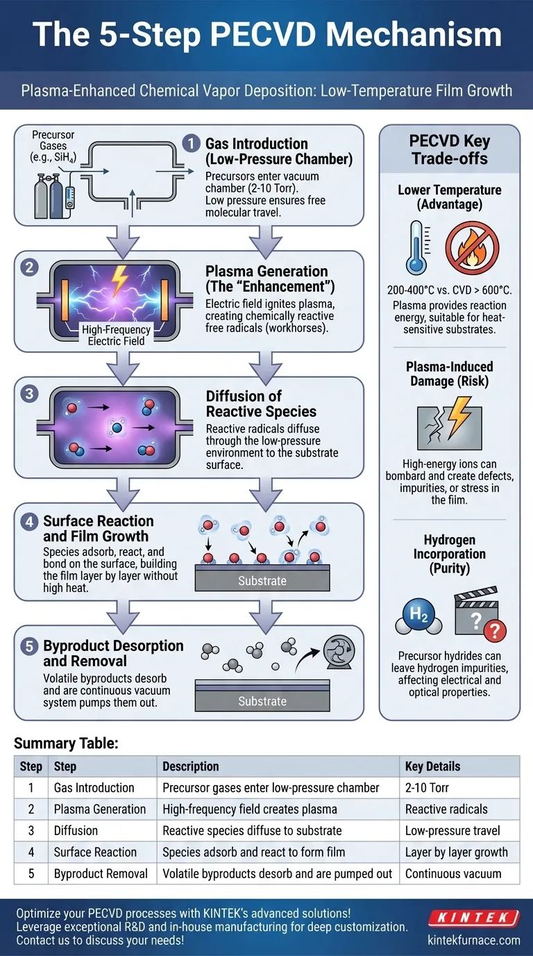
At its core, the Plasma-Enhanced Chemical Vapor Deposition (PECVD) mechanism is a five-step process that begins with introducing reactant gases into a chamber and generating a plasma. This plasma creates highly reactive species that diffuse to a substrate, react on its surface to form a solid film, and release gaseous byproducts that are then removed from the chamber. The use of plasma is the key element that distinguishes this process from other deposition methods.
PECVD leverages the energy of a plasma, not just high temperatures, to drive chemical reactions. This fundamental difference allows for the deposition of high-quality thin films at significantly lower temperatures than traditional Chemical Vapor Deposition (CVD), enabling a much wider range of applications.
The PECVD Process: A Step-by-Step Breakdown
Understanding the PECVD mechanism involves following the journey of precursor molecules as they are transformed from a gas into a solid film. Each step is precisely controlled to achieve the desired film properties.
Step 1: Gas Introduction into a Low-Pressure Chamber
The process begins by introducing carefully measured amounts of reactant gases, known as precursors, into a vacuum chamber.
The chamber is maintained at a low pressure, typically in the range of 2-10 Torr. This low pressure is critical for generating a stable plasma and ensuring the reactant molecules can travel freely to the substrate.
Step 2: Plasma Generation (The "Enhancement")
This is the defining step of PECVD. A high-frequency electric field is applied across the gas in the chamber, stripping electrons from the precursor molecules.
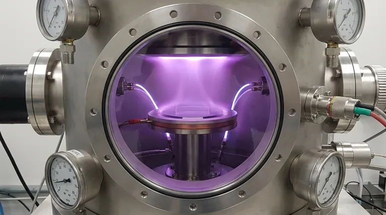
This action ignites a plasma, a partially ionized gas containing ions, electrons, and a high concentration of chemically reactive free radicals. These radicals are the workhorses of the PECVD process.
Step 3: Diffusion of Reactive Species
The highly reactive free radicals and other species created in the plasma do not react in the gas phase. Instead, they diffuse through the low-pressure environment and travel toward the substrate surface.
The path and energy with which these species arrive at the substrate are key parameters that influence the final film's density and stress.
Step 4: Surface Reaction and Film Growth
Once the reactive species reach the substrate, they adsorb onto the surface, meaning they stick to it.
Because these species are already highly energized from the plasma, they can react and bond with the surface (and each other) without requiring high thermal energy. This sequence of adsorption and surface reaction builds the thin film, layer by layer.
Step 5: Byproduct Desorption and Removal
The chemical reactions on the surface often produce unwanted volatile byproducts. These byproduct molecules desorb (detach) from the surface of the growing film.
A continuous vacuum system pumps these gaseous byproducts out of the reaction chamber, keeping the surface clean and allowing the deposition process to continue efficiently.
Understanding the Key Trade-offs
While powerful, the use of plasma introduces specific advantages and challenges that are critical to understand for process control.
The Primary Advantage: Lower Temperature
The main benefit of PECVD is its ability to deposit films at low temperatures (typically 200-400°C), whereas traditional CVD can require 600-1000°C or more.
This is possible because the plasma provides the energy needed to break chemical bonds, a role typically filled by heat. This makes PECVD suitable for temperature-sensitive substrates like plastics or fully fabricated microelectronic devices.
The Inherent Risk: Plasma-Induced Damage
The plasma is not entirely gentle. High-energy ions can bombard the substrate and the growing film, potentially creating defects, impurities, or unwanted stress.
Controlling plasma power and frequency is a delicate balancing act between creating enough reactive species for a good deposition rate and minimizing this damaging bombardment.
The Purity Consideration: Hydrogen Incorporation
Many common PECVD precursors are hydrides (e.g., silane, SiH₄, for silicon dioxide deposition). A common side effect is the incorporation of hydrogen into the final film.
This incorporated hydrogen can affect the film's electrical and optical properties. While sometimes desirable, it is often an impurity that must be minimized through careful process tuning.
Making the Right Choice for Your Goal
Your specific objective determines how you should approach the PECVD process and its parameters.
- If your primary focus is depositing on heat-sensitive materials: PECVD is your ideal choice, as the plasma, not high temperature, provides the necessary energy for the reaction.
- If your primary focus is achieving the highest film purity: You must carefully optimize plasma power to minimize ion damage and consider post-deposition annealing to drive out impurities like hydrogen.
- If your primary focus is maximizing deposition speed: A higher plasma power and gas flow will generally increase the rate of film growth, but this must be balanced against potential impacts on film quality.
Ultimately, mastering PECVD comes from understanding that the plasma is not just an energy source but an active ingredient you can tune to control the final material's properties.
Summary Table:
| Step | Description | Key Details |
|---|---|---|
| 1 | Gas Introduction | Precursor gases enter a low-pressure vacuum chamber (2-10 Torr) |
| 2 | Plasma Generation | High-frequency electric field creates plasma with reactive radicals |
| 3 | Diffusion | Reactive species diffuse to the substrate surface |
| 4 | Surface Reaction | Species adsorb and react to form the solid film |
| 5 | Byproduct Removal | Volatile byproducts desorb and are pumped out |
Optimize your PECVD processes with KINTEK's advanced solutions! Leveraging exceptional R&D and in-house manufacturing, we provide diverse laboratories with high-temperature furnace systems like CVD/PECVD Systems, tailored to your unique experimental needs. Our deep customization capabilities ensure precise control for low-temperature deposition, minimizing plasma-induced damage and enhancing film quality. Contact us today to discuss how our expertise can boost your research and production efficiency!
Visual Guide
Related Products
- Slide PECVD Tube Furnace with Liquid Gasifier PECVD Machine
- RF PECVD System Radio Frequency Plasma Enhanced Chemical Vapor Deposition
- Inclined Rotary Plasma Enhanced Chemical Deposition PECVD Tube Furnace Machine
- Inclined Rotary Plasma Enhanced Chemical Deposition PECVD Tube Furnace Machine
- Multi Heating Zones CVD Tube Furnace Machine for Chemical Vapor Deposition Equipment
People Also Ask
- What are the main advantages of PECVD tube furnaces compared to CVD tube furnaces? Lower Temp, Faster Deposition, and More
- What is plasma in the context of PECVD? Unlock Low-Temperature Thin Film Deposition
- How does a hydrogen reduction environment in an industrial tube furnace facilitate gold-copper alloy microspheres?
- What role does a Tube Furnace play in the CVD growth of carbon nanotubes? Achieve High-Purity CNT Synthesis
- What are the advantages of using a tube furnace CVD system for Cu(111)/graphene? Superior Scalability and Quality


