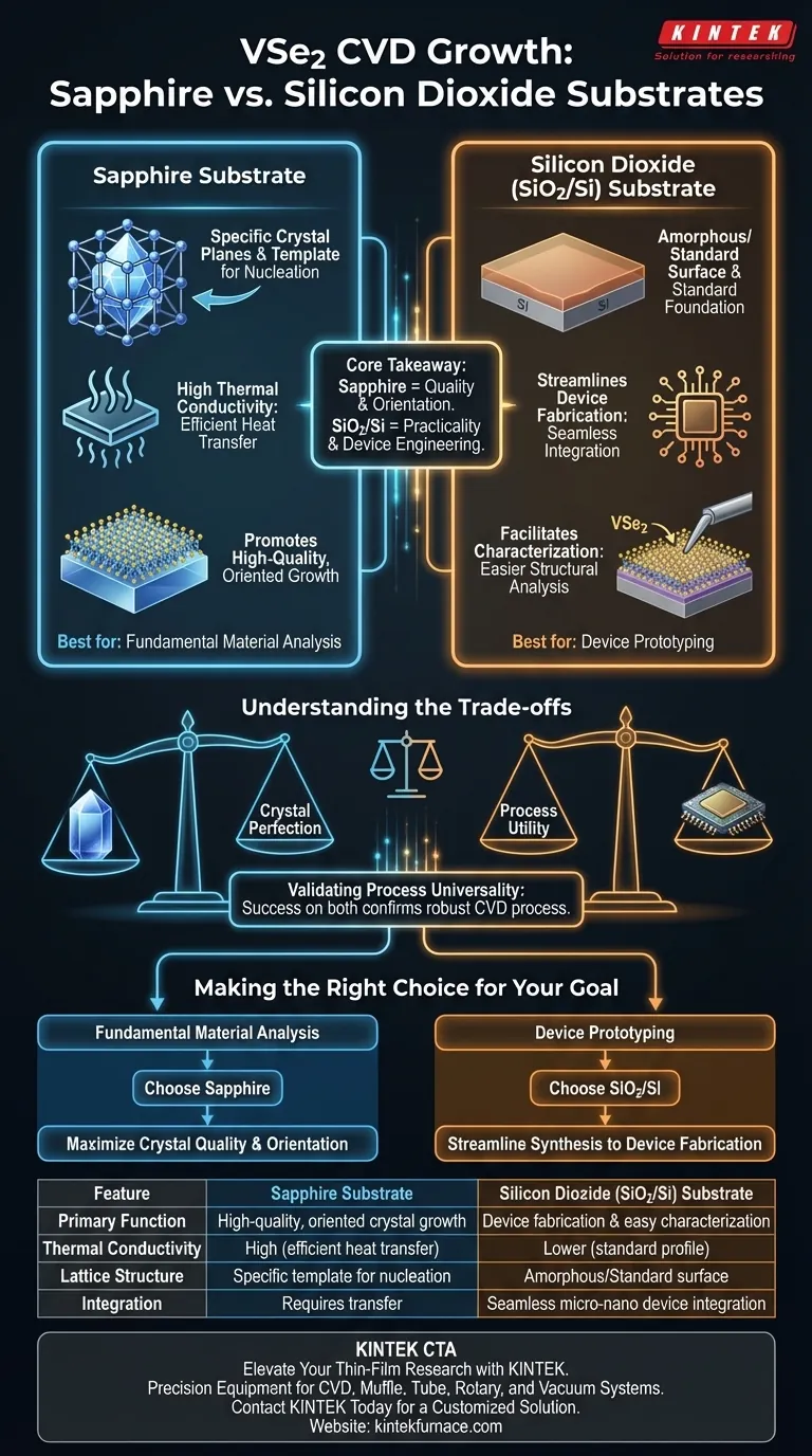
Sapphire substrates are utilized primarily to promote high-quality, oriented crystal growth due to their high thermal conductivity and specific lattice structures. Conversely, silicon dioxide (SiO2/Si) substrates are selected to facilitate seamless integration into micro-nano device fabrication and to allow for easier structural characterization.
Core Takeaway: While sapphire optimizes the physical quality and orientation of VSe2 crystals during synthesis, SiO2/Si is favored for its practical utility in downstream device engineering. Successfully growing VSe2 on both substrate types serves to validate the universality and robustness of the CVD growth process.
The Role of Sapphire in Crystal Synthesis
Leveraging Thermal Properties
Sapphire substrates are characterized by high thermal conductivity.
In a Chemical Vapor Deposition (CVD) environment, this property ensures efficient heat transfer, which is critical for maintaining the stable temperatures required for uniform material deposition.
Achieving Oriented Growth
The surface of a sapphire substrate presents specific crystal plane structures.
These structures act as a template, influencing nucleation and promoting the oriented growth of VSe2. This results in crystals of significantly higher quality compared to those grown on non-crystalline or mismatched surfaces.
The Utility of Silicon Dioxide (SiO2/Si)
Streamlining Device Fabrication
The primary function of SiO2/Si substrates in this context is compatibility.
Because SiO2/Si is the standard foundation for semiconductor technology, growing VSe2 directly on this substrate simplifies the subsequent fabrication of micro-nano devices. It eliminates complex transfer processes often required when moving crystals from a growth substrate to a device substrate.
Facilitating Characterization
SiO2/Si substrates are specifically noted for aiding in structural characterization.
The properties of the substrate make it easier for researchers to analyze the physical structure of the deposited VSe2 material, ensuring that the synthesized layers meet technical specifications.
Understanding the Trade-offs
Quality vs. Applicability
The choice between these substrates represents a trade-off between crystal perfection and process utility.
Sapphire is the superior choice when the primary metric is the intrinsic quality and alignment of the crystal lattice. However, SiO2/Si is superior when the end goal is the rapid development and testing of electronic devices.
Validating Process Universality
Using disparate substrates is not just about choosing one over the other; it is a method of process validation.
By demonstrating that VSe2 can be successfully grown on both the high-performance surface of sapphire and the practical surface of SiO2, researchers confirm that their CVD process is "universal" and not strictly dependent on a specific substrate interaction to work.
Making the Right Choice for Your Goal
To select the correct substrate for your specific VSe2 application, evaluate your immediate objectives:
- If your primary focus is fundamental material analysis: Choose sapphire to maximize crystal quality, orientation, and thermal management during growth.
- If your primary focus is device prototyping: Choose silicon dioxide (SiO2/Si) to streamline the transition from synthesis to micro-nano device fabrication and characterization.
By matching the substrate's functional strengths to your project's phase, you ensure efficiency in both research and application.
Summary Table:
| Feature | Sapphire Substrate | Silicon Dioxide (SiO2/Si) Substrate |
|---|---|---|
| Primary Function | High-quality, oriented crystal growth | Device fabrication & easy characterization |
| Thermal Conductivity | High (efficient heat transfer) | Lower (standard semiconductor profile) |
| Lattice Structure | Specific template for nucleation | Amorphous/Standard surface |
| Integration | Requires transfer for device use | Seamless micro-nano device integration |
| Best Used For | Fundamental material analysis | Rapid prototyping & device engineering |
Elevate Your Thin-Film Research with KINTEK
Precision in VSe2 synthesis starts with the right equipment and the right substrate. Whether you are targeting fundamental crystal analysis on sapphire or streamlining device fabrication on SiO2/Si, KINTEK provides the specialized tools to ensure success.
Backed by expert R&D and manufacturing, we offer high-performance Muffle, Tube, Rotary, Vacuum, and CVD systems, all customizable to your unique research needs. Don't settle for inconsistent growth—partner with KINTEK to achieve professional-grade results in every synthesis cycle.
Contact KINTEK Today for a Customized Solution
Visual Guide
References
- Gangtae Jin. Controlled Vapor-Phase Synthesis of VSe2 via Selenium-Driven Gradual Transformation of Single-Crystalline V2O5 Nanosheets. DOI: 10.3390/nano15070548
This article is also based on technical information from Kintek Furnace Knowledge Base .
Related Products
- Custom Made Versatile CVD Tube Furnace Chemical Vapor Deposition CVD Equipment Machine
- Multi Heating Zones CVD Tube Furnace Machine for Chemical Vapor Deposition Equipment
- Split Chamber CVD Tube Furnace with Vacuum Station CVD Machine
- Cylindrical Resonator MPCVD Machine System for Lab Diamond Growth
- MPCVD Machine System Reactor Bell-jar Resonator for Lab and Diamond Growth
People Also Ask
- Which industries and research fields benefit from CVD tube furnace sintering systems for 2D materials? Unlock Next-Gen Tech Innovations
- What improvements can be made to the bonding force of gate dielectric films using a CVD tube furnace? Enhance Adhesion for Reliable Devices
- How might AI and machine learning enhance CVD tube furnace processes? Boost Quality, Speed, and Safety
- What is a CVD tube furnace and what is its primary function? Discover Precision Thin-Film Deposition
- What customization options are available for CVD tube furnaces? Tailor Your System for Superior Material Synthesis


