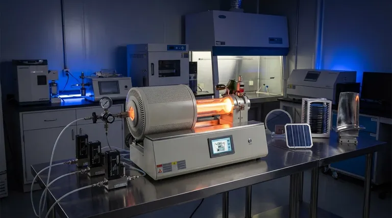
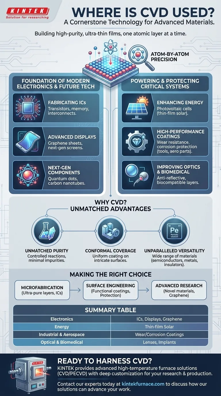
Chemical Vapor Deposition (CVD) is a cornerstone technology used to manufacture the most advanced materials that power our world. Its applications span the electronics, energy, aerospace, and biomedical industries, where it is used to create everything from the microchips in your phone to protective coatings on jet engine parts and biocompatible layers on medical implants.
At its core, CVD is not just about a single application but about a fundamental capability: the ability to build high-purity, ultra-thin films of material one atomic layer at a time. This precise control is why it has become indispensable for nearly every field of modern technology.
The Foundation of Modern Electronics
CVD is the workhorse of the semiconductor industry. The fabrication of complex microelectronics would be impossible without its ability to deposit pristine, functional layers on a microscopic scale.
Fabricating Integrated Circuits
The processors and memory chips that form the brain of every electronic device rely on CVD. It is used to deposit the thin films that create transistors, including active semiconductor layers (like silicon or gallium arsenide), insulating gate dielectrics, and conductive metal interconnects (like tungsten).
Building Advanced Displays
Next-generation displays for televisions and mobile devices leverage materials synthesized via CVD. For example, it is a key method for producing large-area graphene sheets, which promise to enable flexible, transparent, and highly efficient screens.
Enabling Next-Generation Components
The technology is also instrumental in creating novel materials for future electronics. This includes synthesizing quantum dots for more efficient displays and carbon nanotubes for advanced transistors and interconnects.
Powering and Protecting Critical Systems
Beyond microchips, CVD is essential for creating robust and efficient components for energy, industrial, and optical applications. Its value lies in modifying a material's surface to give it entirely new properties.
Enhancing Energy Production
CVD is widely used in the solar industry to manufacture photovoltaic cells. It deposits the thin films of amorphous polysilicon that are responsible for converting sunlight into electricity, directly contributing to the efficiency of solar panels.
Creating High-Performance Coatings
The process can apply exceptionally hard and durable coatings to a variety of surfaces. Synthetic diamond films on cutting tools dramatically increase their lifespan, while specialized coatings on automotive and aerospace parts provide critical resistance to wear and corrosion.
Improving Optical Devices
From everyday sunglasses to specialized scientific instruments, CVD is used to apply thin films that control the reflection and transmission of light. This includes anti-reflective coatings on lenses, UV-blocking layers on architectural glass, and protective layers on optical windows used in harsh environments.
Understanding the Trade-offs: Why CVD is Chosen
CVD is not always the simplest or cheapest method for applying a film, but it is chosen when performance and precision are non-negotiable. Its dominance comes from three key advantages that other techniques cannot easily match.
Unmatched Purity
Because CVD is based on controlled chemical reactions using highly pure precursor gases, the resulting films are exceptionally pure. This is critical in semiconductor manufacturing, where even microscopic impurities can cause a device to fail.
Conformal Coverage
Unlike line-of-sight deposition methods, CVD gases can coat all surfaces of a complex, three-dimensional object with a perfectly uniform film. This "conformal coverage" is essential for ensuring complete protection on intricate parts and for fabricating modern, non-planar transistors.
Unparalleled Versatility
The sheer variety of precursor chemicals available allows CVD to deposit an enormous range of materials. This includes semiconductors (silicon), insulators (oxides, nitrides), and pure metals (tungsten), making it a single, flexible platform for building complex, multi-layered devices.
Making the Right Choice for Your Goal
The decision to use CVD is driven by the specific material properties you need to achieve.
- If your primary focus is microfabrication: CVD is the industry standard for creating the ultra-pure, atomically precise layers required for transistors and integrated circuits.
- If your primary focus is surface engineering: CVD is the ideal choice for adding a high-performance functional coating—like wear resistance, corrosion protection, or biocompatibility—to a component.
- If your primary focus is advanced materials research: CVD provides the fine control needed to synthesize and explore novel materials like graphene, carbon nanotubes, and quantum dots.
Ultimately, Chemical Vapor Deposition is the enabling process that transforms raw materials into high-performance, functional surfaces.
Summary Table:
| Application Area | Key CVD Uses |
|---|---|
| Electronics | Fabricating transistors, memory chips, and advanced displays (e.g., graphene). |
| Energy | Manufacturing thin-film solar cells for photovoltaic panels. |
| Industrial & Aerospace | Applying ultra-hard, wear-resistant coatings on cutting tools and engine parts. |
| Optical & Biomedical | Creating anti-reflective lenses, UV-blocking glass, and biocompatible implant coatings. |
Ready to harness the power of CVD for your research or production?
At KINTEK, we leverage our exceptional R&D and in-house manufacturing to provide advanced high-temperature furnace solutions tailored for CVD and PECVD processes. Whether you are developing next-generation semiconductors, synthesizing novel materials like graphene, or applying high-performance coatings, our product line—including Tube Furnaces, Vacuum & Atmosphere Furnaces, and dedicated CVD/PECVD Systems—is designed to meet your precise requirements. Our strong deep customization capability ensures your unique experimental or production goals are achieved.
Contact our experts today to discuss how our solutions can advance your work.
Visual Guide
Related Products
- Custom Made Versatile CVD Tube Furnace Chemical Vapor Deposition CVD Equipment Machine
- Multi Heating Zones CVD Tube Furnace Machine for Chemical Vapor Deposition Equipment
- HFCVD Machine System Equipment for Drawing Die Nano Diamond Coating
- Split Chamber CVD Tube Furnace with Vacuum Station CVD Machine
- 915MHz MPCVD Diamond Machine Microwave Plasma Chemical Vapor Deposition System Reactor
People Also Ask
- Which industries and research fields benefit from CVD tube furnace sintering systems for 2D materials? Unlock Next-Gen Tech Innovations
- Why are CVD tube furnace sintering systems indispensable for 2D material research and production? Unlock Atomic-Scale Precision
- What are the key application fields of CVD tube furnaces? Unlock Precision in Thin-Film Synthesis
- What are the practical applications of gate media prepared by CVD tube furnaces? Unlock Advanced Electronics and More
- What are the benefits of developing new precursor materials for CVD tube furnaces? Unlock Advanced Thin-Film Synthesis


