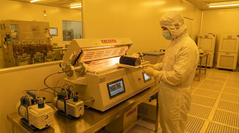
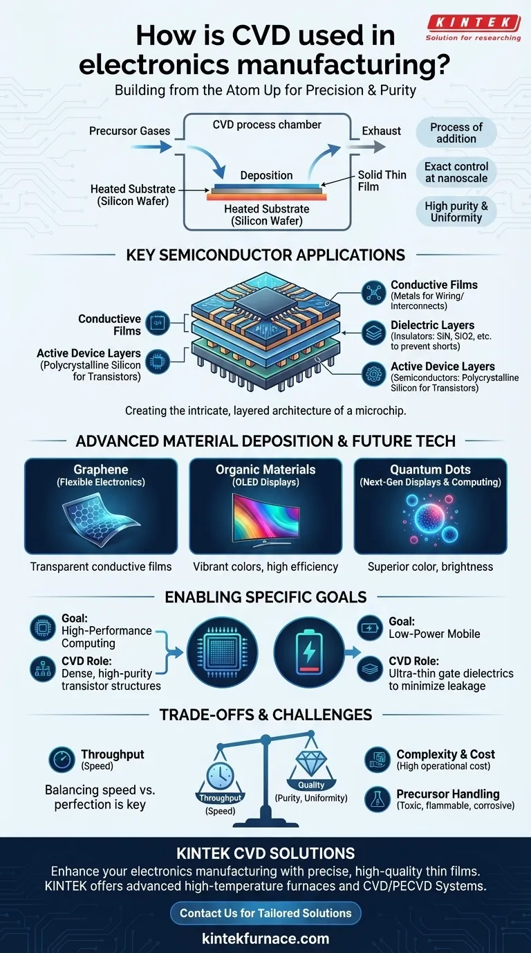
In electronics manufacturing, Chemical Vapor Deposition (CVD) is the foundational process used to build the critical components of a microchip from the atom up. It works by introducing reactant gases into a chamber, which then decompose and deposit a solid, ultra-thin film onto a substrate, such as a silicon wafer. This method is indispensable for creating the high-purity, perfectly uniform layers that form transistors, capacitors, and the wiring that connects them.
At its core, CVD is not just about adding a layer of material. It is about the absolute control it provides over thickness, composition, and purity at the nanoscale, which is the non-negotiable requirement for manufacturing virtually every advanced electronic device today.
The Core Function of CVD: Building from the Atom Up
CVD is a process of addition. It allows fabricators to construct the intricate, layered architecture of a semiconductor device with incredible precision, forming the building blocks of modern computing.
What is Chemical Vapor Deposition?
At its simplest, CVD involves a chemical reaction that starts with a gas and ends with a solid. A substrate, typically a silicon wafer, is placed in a reaction chamber. Specific gases, known as precursors, are then introduced. When these gases react or decompose on the hot surface of the substrate, they form a solid thin film, with the byproducts being exhausted from the chamber.
Why Precision is Non-Negotiable
Modern microchips contain billions of transistors, each with features measured in nanometers. For these components to function correctly, the layers they are made of—insulators, conductors, and semiconductors—must have exact thicknesses and be free of impurities. CVD provides this level of control, enabling the fabrication of these complex nanoscale patterns.
Key Benefits: Purity and Uniformity
The performance of an electronic device is directly tied to the quality of its material layers. CVD excels at producing films that are both highly pure and exceptionally uniform across the entire surface of a wafer. This consistency is critical for achieving high manufacturing yields and reliable device performance.
Key Applications in Semiconductor Fabrication
CVD is not a single-use technique; it is a versatile toolset used multiple times during the creation of an integrated circuit to deposit different types of materials.
Depositing Dielectric Layers
Dielectric materials are electrical insulators. CVD is used to deposit films like silicon nitride and silicon dioxide to isolate conductive components from one another, prevent electrical "short circuits," and protect the device from the environment. These layers are fundamental to creating functional transistors and capacitors.
Creating Conductive Films
While photolithography defines the patterns for wiring, CVD is used to deposit the conductive materials themselves. It can create thin films of metals that serve as the "interconnects" or wiring between millions of transistors, forming the complex circuits that allow the chip to perform calculations.
Forming Active Device Layers
Perhaps the most critical role of CVD is depositing the semiconductor layers that form the active parts of a transistor. This includes depositing layers of polycrystalline silicon or other semiconductor materials that control the flow of electricity, which is the very essence of a transistor's function as a switch.
Pushing the Boundaries: Advanced Material Deposition
While central to traditional silicon chips, CVD's versatility extends to cutting-edge materials that are enabling the next generation of electronics.
Graphene for Flexible Electronics
CVD is one of the primary methods for growing large, high-quality, single-atom-thick sheets of graphene. This capability is paving the way for transparent conductive films used in flexible displays, wearable sensors, and other novel electronic devices.
Organic Materials for OLED Displays
Certain variations of CVD are used to deposit the thin layers of organic compounds that make up Organic Light Emitting Diodes (OLEDs). The precise layering of these materials is what allows OLED screens to produce vibrant colors with high efficiency.
Quantum Dots for Next-Gen Displays
CVD techniques are being adapted to deposit quantum dots, which are semiconductor nanocrystals. These materials offer superior color accuracy and brightness for next-generation displays and also have applications in biomedical imaging and quantum computing.
Understanding the Trade-offs and Challenges
Despite its power, CVD is a highly sophisticated process with inherent complexities that manufacturers must manage.
Process Complexity and Cost
CVD reactors are expensive, complex systems that require precise control over temperature, pressure, and gas flow. Maintaining these systems and ensuring process repeatability represents a significant operational cost and technical challenge.
Precursor Material Handling
The precursor gases used in CVD can be highly toxic, flammable, or corrosive. Handling, storing, and delivering these materials safely requires extensive infrastructure and rigorous safety protocols, adding to the overall cost and complexity of fabrication.
Throughput vs. Quality
There is often a trade-off between the speed of deposition (throughput) and the quality of the resulting film. Processes that produce the highest-quality films may be slower, creating a bottleneck in high-volume manufacturing. Engineers must constantly balance these factors to meet production targets.
How CVD Enables Specific Electronic Goals
Your engineering goal will determine which aspect of CVD technology is most critical to your success.
- If your primary focus is high-performance computing: CVD is essential for creating the dense, high-purity transistor structures with flawless insulating layers that define processing power.
- If your primary focus is next-generation displays: CVD and its variants are critical for depositing the organic or quantum dot layers that produce vibrant, efficient screens.
- If your primary focus is low-power mobile devices: The ability of CVD to create perfect, ultra-thin gate dielectrics is key to minimizing power leakage in transistors.
- If your primary focus is flexible or novel electronics: Advanced CVD methods are the key to integrating innovative materials like graphene into non-traditional form factors.
Ultimately, Chemical Vapor Deposition is the invisible architecture behind the digital world, enabling the creation of complex electronic devices one atomic layer at a time.
Summary Table:
| Application | Key Materials | Benefits |
|---|---|---|
| Dielectric Layers | Silicon Nitride, Silicon Dioxide | Electrical insulation, prevents short circuits |
| Conductive Films | Metals (e.g., for interconnects) | Forms wiring between transistors |
| Active Device Layers | Polycrystalline Silicon | Creates transistor switches |
| Advanced Materials | Graphene, Organic Compounds, Quantum Dots | Enables flexible displays, OLEDs, and next-gen screens |
Ready to enhance your electronics manufacturing with precise, high-quality thin films? KINTEK leverages exceptional R&D and in-house manufacturing to provide advanced high-temperature furnace solutions, including CVD/PECVD Systems. Our product line—featuring Muffle, Tube, Rotary Furnaces, Vacuum & Atmosphere Furnaces, and more—is complemented by strong deep customization capabilities to meet your unique experimental needs. Contact us today to discuss how our tailored solutions can drive your innovation forward!
Visual Guide
Related Products
- Custom Made Versatile CVD Tube Furnace Chemical Vapor Deposition CVD Equipment Machine
- Split Chamber CVD Tube Furnace with Vacuum Station CVD Machine
- Multi Heating Zones CVD Tube Furnace Machine for Chemical Vapor Deposition Equipment
- Slide PECVD Tube Furnace with Liquid Gasifier PECVD Machine
- Controlled Inert Nitrogen Hydrogen Atmosphere Furnace
People Also Ask
- How does CVD tube furnace sintering enhance graphene growth? Achieve Superior Crystallinity and High Electron Mobility
- Why are CVD tube furnace sintering systems indispensable for 2D material research and production? Unlock Atomic-Scale Precision
- Which industries and research fields benefit from CVD tube furnace sintering systems for 2D materials? Unlock Next-Gen Tech Innovations
- What is a CVD tube furnace and what is its primary function? Discover Precision Thin-Film Deposition
- What improvements can be made to the bonding force of gate dielectric films using a CVD tube furnace? Enhance Adhesion for Reliable Devices


