In the field of material preparation, Chemical Vapor Deposition (CVD) furnaces are primarily used for two critical processes: depositing ultra-thin films onto a surface and synthesizing advanced nanomaterials. By precisely controlling a chemical reaction in a high-temperature, vacuum environment, these furnaces can create highly pure, uniform materials that are foundational to the semiconductor, energy, and nanotechnology sectors.
The true value of a CVD furnace lies not just in its ability to create materials, but in its precise control over their fundamental building blocks. By manipulating gas, temperature, and pressure, it enables the atomic-level engineering required for today's most advanced technologies.
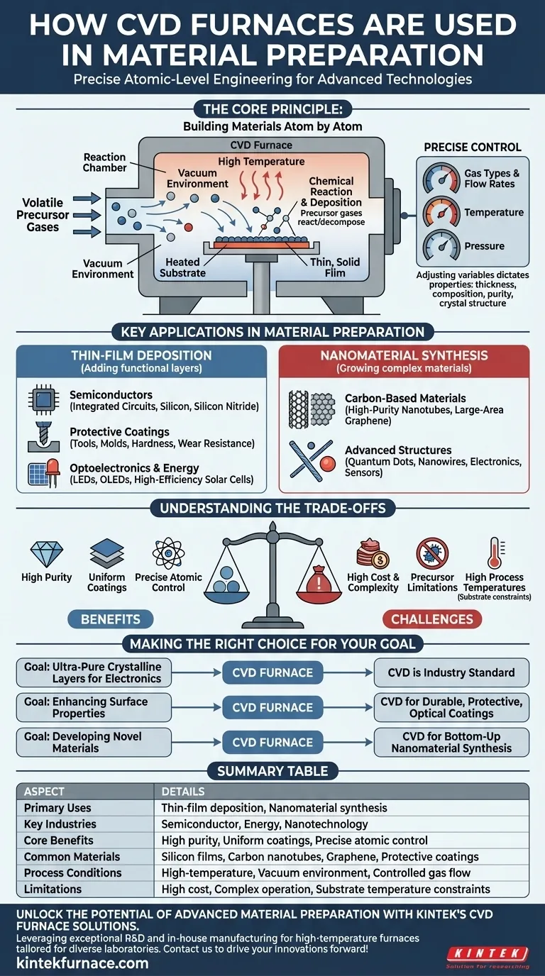
The Core Principle: Building Materials Atom by Atom
CVD is a process that builds solid materials from the ground up, one molecule at a time. Understanding this principle is key to seeing its value.
What is Chemical Vapor Deposition?
The process begins with one or more volatile precursor gases being introduced into the furnace's reaction chamber.
Inside the chamber, a substrate (the material to be coated) is heated to a high temperature. This heat causes the precursor gases to react or decompose, depositing a thin, solid film onto the substrate's surface.
The Power of Precise Control
A CVD system’s strength is its ability to meticulously control every variable of this reaction. By adjusting the gas types, flow rates, temperature, and pressure, operators can dictate the final material's properties.
This control allows for the creation of films with specific thickness, composition, purity, and crystal structure, making it an engineering tool rather than a simple heating chamber.
Key Applications in Material Preparation
The precision of CVD enables its use in two main areas: adding layers to existing objects (films) and creating entirely new, tiny structures (nanomaterials).
Thin-Film Deposition
This is the most common application, where a functional layer is added to a substrate.
- Semiconductors: CVD is essential for manufacturing integrated circuits. It is used to deposit critical layers like silicon, silicon nitride, and the gate media in advanced MOSFET transistors.
- Protective Coatings: Hard coatings are deposited on tools and molds to dramatically improve their hardness and wear resistance, extending their operational life.
- Optoelectronics & Energy: The technology is used to create the thin films necessary for manufacturing LEDs, OLEDs, and high-efficiency thin-film solar cells.
Nanomaterial Synthesis
CVD is also used to "grow" complex materials with unique properties from the bottom up.
- Carbon-Based Materials: It is a primary method for synthesizing high-purity carbon nanotubes and large-area graphene sheets, materials with extraordinary strength and electrical conductivity.
- Advanced Structures: The process can produce other nanomaterials like quantum dots and nanowires, which are critical components in next-generation electronics and sensors.
Understanding the Trade-offs
While powerful, CVD is not a universal solution. Its effectiveness is balanced by important practical considerations.
High Cost and Complexity
CVD systems require vacuum chambers, high-purity precursor gases, and sophisticated control systems. This makes them more complex and expensive to operate than many other material preparation techniques.
Precursor Material Limitations
The entire process depends on the availability of suitable precursor gases that are volatile and decompose cleanly at manageable temperatures. Finding the right precursor for a desired film material can be a significant challenge.
High Process Temperatures
Many CVD processes require very high temperatures to initiate the chemical reaction. This can limit the types of substrate materials that can be used, as they must be able to withstand the heat without melting, warping, or degrading.
Making the Right Choice for Your Goal
The decision to use a CVD furnace depends entirely on the material properties you need to achieve.
- If your primary focus is creating ultra-pure, crystalline layers for electronics: CVD is the industry standard for depositing the critical semiconductor and dielectric films required for integrated circuits.
- If your primary focus is enhancing the surface properties of a component: CVD is a leading choice for applying durable protective, optical, or wear-resistant coatings that cannot be achieved by other means.
- If your primary focus is developing novel materials with unique structures: CVD provides the bottom-up control needed to synthesize advanced nanomaterials like carbon nanotubes and graphene.
Ultimately, a CVD furnace is a foundational tool for engineering materials from the molecular level upwards, enabling the innovations that define modern technology.
Summary Table:
| Aspect | Details |
|---|---|
| Primary Uses | Thin-film deposition, Nanomaterial synthesis |
| Key Industries | Semiconductor, Energy, Nanotechnology |
| Core Benefits | High purity, Uniform coatings, Precise atomic control |
| Common Materials | Silicon films, Carbon nanotubes, Graphene, Protective coatings |
| Process Conditions | High-temperature, Vacuum environment, Controlled gas flow |
| Limitations | High cost, Complex operation, Substrate temperature constraints |
Unlock the potential of advanced material preparation with KINTEK's CVD furnace solutions. Leveraging exceptional R&D and in-house manufacturing, we provide high-temperature furnaces, including CVD/PECVD systems, tailored for diverse laboratories. Our deep customization capabilities ensure precise alignment with your unique experimental needs—whether for semiconductor development, energy applications, or nanomaterial synthesis. Contact us today to discuss how our reliable, high-performance furnaces can drive your innovations forward!
Visual Guide
Related Products
- Custom Made Versatile CVD Tube Furnace Chemical Vapor Deposition CVD Equipment Machine
- Split Chamber CVD Tube Furnace with Vacuum Station CVD Machine
- Multi Heating Zones CVD Tube Furnace Machine for Chemical Vapor Deposition Equipment
- Slide PECVD Tube Furnace with Liquid Gasifier PECVD Machine
- Controlled Inert Nitrogen Hydrogen Atmosphere Furnace
People Also Ask
- What improvements can be made to the bonding force of gate dielectric films using a CVD tube furnace? Enhance Adhesion for Reliable Devices
- How does CVD tube furnace sintering enhance graphene growth? Achieve Superior Crystallinity and High Electron Mobility
- What temperature range do standard CVD tube furnaces operate at? Unlock Precision for Your Material Deposition
- Which industries and research fields benefit from CVD tube furnace sintering systems for 2D materials? Unlock Next-Gen Tech Innovations
- How might AI and machine learning enhance CVD tube furnace processes? Boost Quality, Speed, and Safety


