A high-vacuum environment is strictly necessary to prevent contamination and oxidation of the metal vapor during the thermal evaporation process. By removing air molecules, the system ensures that gold atoms can travel without interference and condense uniformly onto the target area. This precision creates a 200 nm thick electrode layer with the high conductivity and low contact resistance required for efficient solar cell operation.
Creating a pristine path for deposition is critical for device physics, not just cleanliness. A high-vacuum state maximizes the mean free path of gold atoms, guaranteeing a contaminant-free, low-resistance interface that is essential for collecting electrical current.
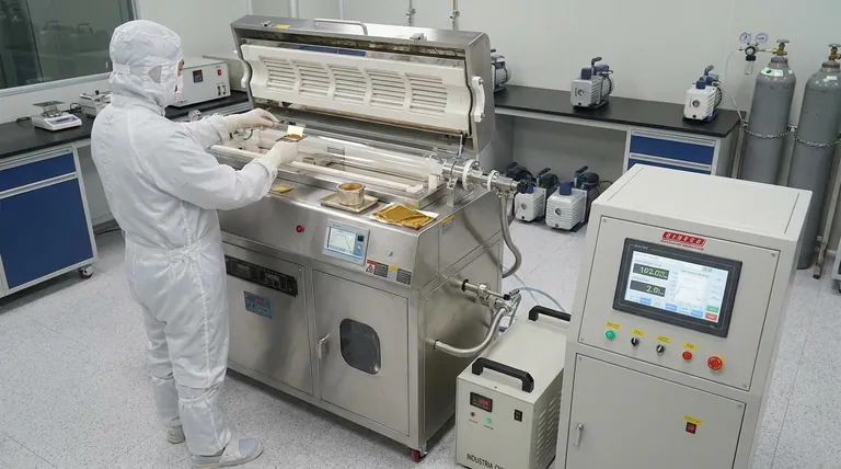
The Physics of Vacuum Deposition
Preventing Molecular Interference
In a standard atmosphere, gas molecules are densely packed. If gold were evaporated under these conditions, the metal atoms would constantly collide with air molecules.
High vacuum solves this by significantly increasing the mean free path—the distance a particle travels before colliding with another. This allows the evaporated gold atoms to travel directly and directionally to the device surface without scattering.
Eliminating Contamination and Oxidation
Gold is a noble metal, but the deposition process involves high energy states where impurities can easily be trapped.
A high-vacuum environment effectively removes reactive gases and impurities from the chamber. This prevents the inclusion of impurity atoms and protects the gold vapor from oxidation, which would otherwise degrade the quality of the material before it even reaches the solar cell.
Impact on Solar Cell Performance
Minimizing Contact Resistance
The primary goal of the gold electrode is to extract current from the solar cell with minimal loss.
The high-vacuum process results in a deposited layer—typically around 200 nm thick—that exhibits extremely low contact resistance. This ensures that the energy generated by the solar cell is not lost as heat at the electrode interface.
Ensuring Uniformity and Adhesion
Electrical performance relies on the physical integrity of the electrode.
Vacuum deposition allows for a highly uniform condensation of gold atoms. This uniformity leads to superior adhesion to the underlying hole transport layer, creating a high-quality ohmic contact that remains stable during operation.
Understanding the Trade-offs
Equipment Complexity and Cost
While high vacuum is essential for performance, it introduces significant logistical challenges.
Achieving pressures low enough for thermal evaporation requires sophisticated pumping systems and robust chamber construction. This increases both the capital cost of the equipment and the maintenance requirements compared to non-vacuum coating methods.
Process Throughput Limitations
The physics of vacuum systems impose time constraints.
Evacuating a chamber to the necessary high-vacuum state takes time, which can limit the throughput of the manufacturing process. This makes the technique excellent for high-performance prototypes but challenging to scale for rapid, low-cost mass production.
Making the Right Choice for Your Goal
To achieve the best results in solar cell fabrication, consider how the deposition environment aligns with your specific performance targets.
- If your primary focus is Electrical Efficiency: Prioritize high-vacuum levels to ensure the lowest possible contact resistance and a pure, 200 nm conductive layer.
- If your primary focus is Device Longevity: Rely on the vacuum process to maximize adhesion, preventing electrode delamination over time.
Control over the vacuum environment is the single most critical factor in transitioning from a theoretical design to a high-functioning prototype.
Summary Table:
| Feature | High-Vacuum Deposition Impact |
|---|---|
| Mean Free Path | Increased; gold atoms travel without air molecular interference |
| Purity | Prevents oxidation and inclusion of reactive gas impurities |
| Resistance | Delivers low contact resistance for efficient current collection |
| Layer Quality | Ensures uniform 200nm thickness and superior adhesion |
| Performance | Essential for high-efficiency, stable solar cell prototypes |
Elevate Your Thin-Film Research with KINTEK
Precision in the deposition of gold electrodes requires uncompromising vacuum control. KINTEK provides industry-leading thermal evaporation systems designed specifically for the rigorous demands of solar cell fabrication and material science.
Backed by expert R&D and manufacturing, we offer a comprehensive range of customizable lab solutions, including Vacuum, CVD, Muffle, and Tube systems tailored to your unique research needs. Ensure your prototypes achieve maximum conductivity and durability with equipment built for excellence.
Ready to optimize your lab's deposition quality? Contact us today to find your perfect solution!
References
- Iván Caño, Edgardo Saucedo. Novel synthesis of semiconductor chalcohalide anti-perovskites by low-temperature molecular precursor ink deposition methodologies. DOI: 10.1039/d3tc04410f
This article is also based on technical information from Kintek Furnace Knowledge Base .
Related Products
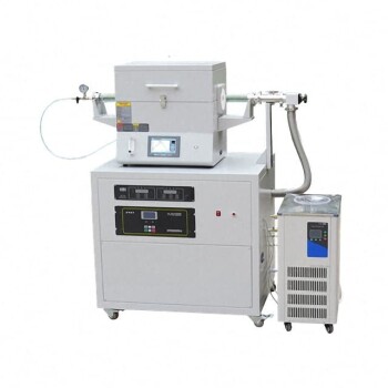
- Multi Heating Zones CVD Tube Furnace Machine for Chemical Vapor Deposition Equipment
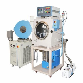
- Split Chamber CVD Tube Furnace with Vacuum Station CVD Machine
- 1700℃ Controlled Inert Nitrogen Atmosphere Furnace
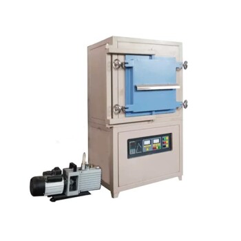
- Vacuum Heat Treat Sintering and Brazing Furnace
- Vacuum Dental Porcelain Sintering Furnace for Dental Laboratories
People Also Ask
- Why are advanced materials and composites important? Unlock Next-Gen Performance in Aerospace, Auto, and More
- What are the advantages of CVD tube furnace sintering systems? Achieve Superior Material Control and Purity
- What is the process for synthesizing transition metal dichalcogenides (TMDs) using CVD tube furnaces? Master High-Quality Thin Film Growth
- What functions does glucose perform in lithium-ion sieve synthesis? Enhance Carbothermal Reduction for LiMnO2 Purity
- What are the practical applications of gate media prepared by CVD tube furnaces? Unlock Advanced Electronics and More

