The 1000 °C pre-annealing treatment acts as a critical surface preparation step designed to transform ordinary copper foil into a high-quality template for growth. This thermal process simultaneously cleans the surface and restructures the metal's internal grain structure. By doing so, it creates the specific physical conditions necessary for the successful heteroepitaxial growth of amorphous-crystalline mixed boron nitride (acm-BN).
Achieving high-performance acm-BN thin films is impossible without a pristine substrate. The 1000 °C pre-annealing step serves as the foundation of the process, ensuring the copper foil is chemically clean and physically ordered to support uniform crystalline growth.
Mechanisms of Substrate Optimization
Elimination of Surface Impurities
Standard copper foils naturally develop an oxide layer when exposed to air. The 1000 °C treatment effectively eliminates this surface oxide layer.
This ensures that the subsequent growth of boron nitride occurs directly on the metallic copper rather than on an unstable oxide interface, which is essential for chemical consistency.
Inducing Grain Growth
Beyond surface cleaning, the high thermal energy induces grain growth within the copper foil.
This restructuring merges smaller, disordered grains into larger, more stable domains. This reduction in grain boundaries is crucial for creating a more uniform substrate across larger areas.
Creating a Stepped Surface Structure
The combination of oxide removal and grain growth results in the formation of a flat, stepped surface structure.
This specific morphology is not merely a side effect; it provides the physical "lock-and-key" mechanism required for heteroepitaxy. The steps guide the atomic alignment of the depositing material.
The Impact on Material Quality
Establishing a Foundation for Heteroepitaxy
The treated copper provides a high-quality physical foundation for heteroepitaxial growth.
In this context, heteroepitaxy refers to the deposition of a crystalline material (BN) onto a different material (Cu) where the crystal lattice of the layer matches the substrate.
Enhancing Crystalline Uniformity
The ultimate goal of this pre-treatment is to improve the quality and uniformity of the crystalline regions within the acm-BN film.
By standardizing the substrate surface, the process ensures that the crystalline domains of the boron nitride grow consistently, reducing defects in the final thin film.
Operational Considerations and Trade-offs
Proximity to Melting Point
Copper has a melting point of approximately 1085 °C. Annealing at 1000 °C operates dangerously close to the material's thermal limit.
This requires precise temperature control. A slight overshoot in temperature could melt the foil, destroying the substrate entirely rather than organizing it.
Thermal Budget and Complexity
Introducing a high-temperature step increases the energy requirements and complexity of the fabrication process.
While necessary for quality, this treatment demands robust equipment capable of maintaining 1000 °C while strictly controlling the atmosphere to prevent immediate re-oxidation during the process.
Making the Right Choice for Your Goal
To maximize the effectiveness of the acm-BN growth process, align your process parameters with your specific quality targets:
- If your primary focus is interface purity: Ensure the annealing environment is strictly controlled to facilitate the complete removal of the oxide layer without introducing new contaminants.
- If your primary focus is crystalline uniformity: Prioritize the stability of the 1000 °C temperature hold to allow sufficient time for maximal grain growth and surface flattening.
The success of the acm-BN film is determined before growth even begins, relying entirely on the rigorous preparation of the copper foundation.
Summary Table:
| Mechanism | Action Taken | Benefit for acm-BN Growth |
|---|---|---|
| Surface Cleaning | Eliminates copper oxide layers | Ensures chemical consistency at the metal interface |
| Grain Growth | Merges small grains into larger domains | Reduces grain boundaries for better substrate stability |
| Surface Morphology | Creates a flat, stepped structure | Provides the physical template for heteroepitaxy |
| Crystalline Control | Standardizes substrate foundation | Enhances the uniformity and quality of BN crystalline regions |
Elevate Your Material Research with KINTEK
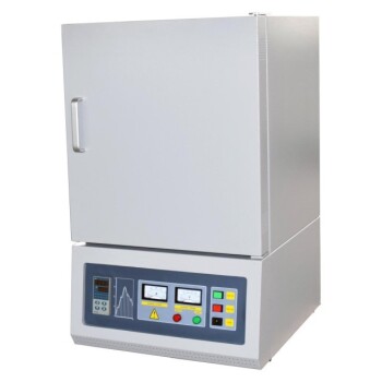
Precision is paramount when operating near the thermal limits of copper. Backed by expert R&D and manufacturing, KINTEK offers high-performance CVD systems, vacuum furnaces, and lab high-temp furnaces designed to maintain the rigorous temperature stability required for 1000 °C pre-annealing and heteroepitaxial growth. Whether you are optimizing acm-BN films or developing next-generation substrates, our customizable solutions ensure uniform results and pristine surface preparation.
Ready to achieve superior crystalline uniformity? Contact our experts today to find the perfect furnace for your laboratory needs!
References
- Synthesis of Amorphous‐Crystalline Mixture Boron Nitride for Balanced Resistive Switching Operation. DOI: 10.1002/smll.202503877
This article is also based on technical information from Kintek Furnace Knowledge Base .
Related Products
- Custom Made Versatile CVD Tube Furnace Chemical Vapor Deposition CVD Equipment Machine
- Multi Heating Zones CVD Tube Furnace Machine for Chemical Vapor Deposition Equipment
- Inclined Rotary Plasma Enhanced Chemical Deposition PECVD Tube Furnace Machine
- HFCVD Machine System Equipment for Drawing Die Nano Diamond Coating
- Slide PECVD Tube Furnace with Liquid Gasifier PECVD Machine
People Also Ask
- Which industries and research fields benefit from CVD tube furnace sintering systems for 2D materials? Unlock Next-Gen Tech Innovations
- How does CVD tube furnace sintering enhance graphene growth? Achieve Superior Crystallinity and High Electron Mobility
- What are the practical applications of gate media prepared by CVD tube furnaces? Unlock Advanced Electronics and More
- Why are CVD tube furnace sintering systems indispensable for 2D material research and production? Unlock Atomic-Scale Precision
- What is the working principle of a CVD tube furnace? Achieve Precise Thin Film Deposition for Your Lab