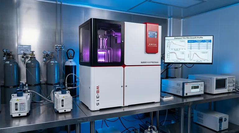
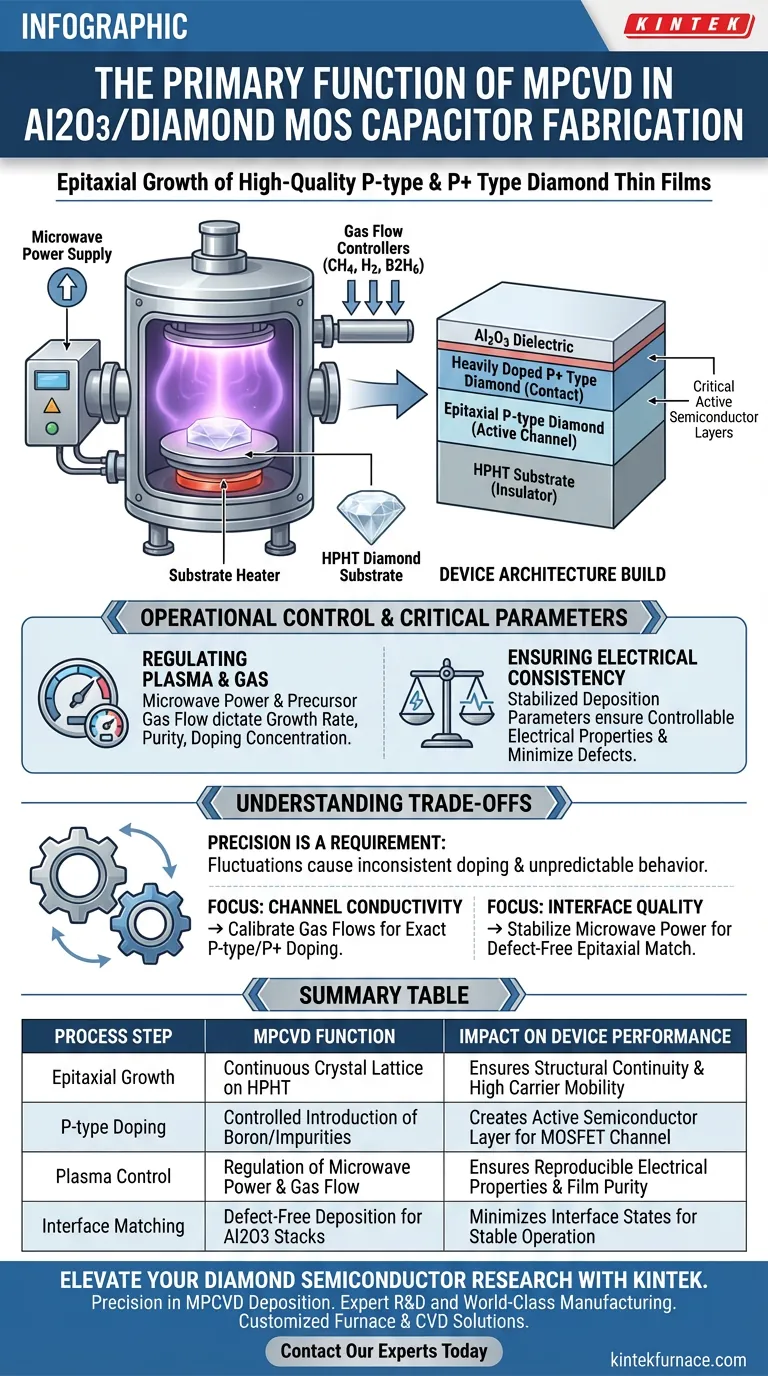
The primary function of a Microwave Plasma Chemical Vapor Deposition (MPCVD) system in this context is to epitaxially grow high-quality p-type and heavily doped p+ type diamond thin films onto High-Pressure High-Temperature (HPHT) single-crystal diamond substrates. This process is essential for creating the active semiconductor layers required for the device's operation.
MPCVD serves as the foundational fabrication step for diamond-based electronics, transforming a raw substrate into a functional semiconductor. By precisely controlling the growth environment, it defines the specific doping profiles necessary for the MOSFET channel to conduct electricity effectively.
The Role of MPCVD in Device Architecture
Epitaxial Growth on HPHT Substrates
The MPCVD system functions as a high-precision deposition tool. Its specific task is to grow new layers of diamond directly onto an existing HPHT single-crystal diamond substrate.
Because this process is epitaxial, the new layers continue the crystal lattice of the substrate perfectly. This ensures structural continuity, which is vital for high-performance electronic devices.
Creating Specific Doping Profiles
A raw diamond substrate is typically an electrical insulator. To function as a semiconductor, it must be doped.
The MPCVD system introduces specific impurities during the growth phase to create p-type and heavily doped p+ type layers. This ability to tune conductivity at the atomic level is what makes the fabrication of complex devices like capacitors and transistors possible.
Forming the Core MOSFET Channel
The layers grown by the MPCVD system are not merely structural coatings; they form the active region of the device.
The reference explicitly notes that these high-quality epitaxial layers serve as the core semiconductor material for MOSFET channels. Without this specific MPCVD step, there is no channel for electrons (or holes) to flow through, rendering the device non-functional.
Operational Control and Critical Parameters
Regulating Microwave Power and Gas Flow
The quality of the diamond film depends entirely on the stability of the plasma environment.
The MPCVD system allows for granular control over microwave power and precursor gas flow rates. Regulating these variables dictates the growth rate, purity, and doping concentration of the final film.
Ensuring Electrical Consistency
The ultimate goal of the MPCVD process is reproducibility. By stabilizing the deposition parameters, the system ensures the grown layers have controllable electrical properties.
This consistency is required to minimize defects that would otherwise degrade the performance of the Al2O3/diamond MOS capacitor stack.
Understanding the Trade-offs
The Necessity of Precision
While MPCVD allows for high-quality growth, it is highly sensitive to parameter fluctuations. The "precise control" mentioned in the reference is not a luxury; it is a requirement.
If microwave power or gas flow deviates, the doping concentration will become inconsistent. This results in a MOSFET channel with unpredictable electrical behavior, compromising the entire device.
Making the Right Choice for Your Goal
When utilizing MPCVD for diamond MOS capacitor fabrication, your operational focus should shift based on your specific requirements:
- If your primary focus is channel conductivity: Prioritize the precise calibration of precursor gas flows to achieve the exact p-type and p+ doping concentrations required.
- If your primary focus is interface quality: Focus on the stability of microwave power to ensure a defect-free epitaxial match with the HPHT substrate.
Success in this fabrication step relies on using the MPCVD system not just to grow diamond, but to engineer specific electrical properties through strict process control.
Summary Table:
| Process Step | MPCVD Function | Impact on Device Performance |
|---|---|---|
| Epitaxial Growth | Continuous crystal lattice formation on HPHT substrates | Ensures structural continuity and high carrier mobility |
| P-type Doping | Controlled introduction of boron/impurities | Creates the active semiconductor layer for the MOSFET channel |
| Plasma Control | Regulation of microwave power & gas flow | Ensures reproducible electrical properties and film purity |
| Interface Matching | Defect-free deposition for Al2O3 stacks | Minimizes interface states for stable capacitor operation |
Elevate Your Diamond Semiconductor Research with KINTEK
Precision in MPCVD deposition is the difference between a failing device and a high-performance Al2O3/diamond MOS capacitor. Backed by expert R&D and world-class manufacturing, KINTEK provides industry-leading Microwave Plasma CVD systems, alongside our Muffle, Tube, and Vacuum furnace solutions. Whether you are engineering p-type doping profiles or complex epitaxial layers, our systems are fully customizable to meet your unique lab requirements.
Ready to achieve superior film quality? Contact our technical experts today to discuss your custom furnace or CVD needs.
Visual Guide
References
- Xufang Zhang, Norio Tokuda. Impact of water vapor annealing treatments on Al2O3/diamond interface. DOI: 10.1063/5.0188372
This article is also based on technical information from Kintek Furnace Knowledge Base .
Related Products
- 915MHz MPCVD Diamond Machine Microwave Plasma Chemical Vapor Deposition System Reactor
- MPCVD Machine System Reactor Bell-jar Resonator for Lab and Diamond Growth
- Cylindrical Resonator MPCVD Machine System for Lab Diamond Growth
- RF PECVD System Radio Frequency Plasma Enhanced Chemical Vapor Deposition
- Slide PECVD Tube Furnace with Liquid Gasifier PECVD Machine
People Also Ask
- What are the main components of an MPCVD machine? Unlock the Secrets of Diamond Synthesis
- What are the essential components of an MPCVD reactor system? Build a Pristine Environment for High-Purity Materials
- What is the purpose of a microwave plasma chemical vapor deposition system? Grow High-Purity Diamonds and Advanced Materials
- What is the MPCVD method and why is it considered effective for diamond deposition? Superior Purity & High Growth Rates
- What is the basic principle of operation for the microwave plasma chemical vapor deposition system? Unlock High-Purity Material Growth


