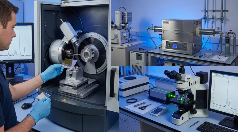
To accurately determine the quality of films from Microwave Plasma-Enhanced Chemical Vapor Deposition (MPCVD), a suite of complementary characterization techniques is required. The most common methods are X-ray diffraction (XRD) for analyzing crystal structure, Raman spectroscopy for chemical purity, scanning electron microscopy (SEM) for surface morphology, and ellipsometry for thickness and optical constants. No single technique is sufficient; they are used together to build a comprehensive understanding of the film's properties.
True film quality is not a single metric but a multidimensional assessment. The key is to select a combination of techniques that provides a complete picture of the film's structural integrity, chemical purity, and surface uniformity, directly linking these properties back to the deposition process itself.
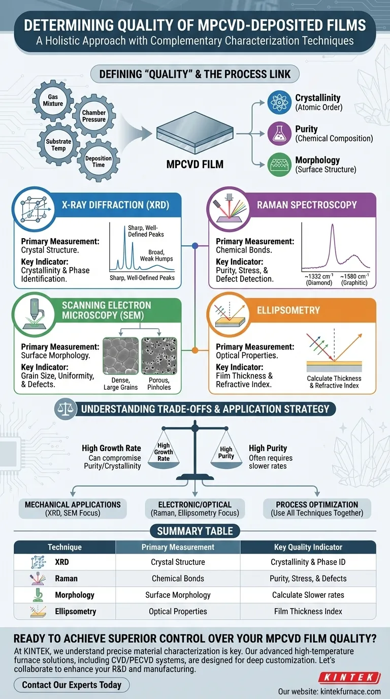
Defining "Quality" in MPCVD Films
The MPCVD process involves using microwave energy to create a plasma from precursor gases, which then decompose and deposit a solid film onto a substrate. The final quality is a direct result of how well this process is controlled.
What "Quality" Really Means
A "high-quality" film is one that meets the specific requirements for its intended application. This goes far beyond simply being a uniform layer.
Key quality indicators include crystallinity (how ordered the atoms are), purity (the absence of unwanted chemical phases or contaminants), and morphology (the physical structure of the film's surface and grains).
The Link to Deposition Parameters
The quality of the final film is dictated by the precise control of deposition parameters. The gas mixture, chamber pressure, substrate temperature, and deposition time all interact to determine the film's final characteristics.
Understanding how to measure the film's properties is the first step toward optimizing these parameters to achieve a desired outcome.
Core Characterization Techniques Explained
Each technique provides a different piece of the puzzle. Using them in concert allows you to correlate process inputs with material outputs.
X-ray Diffraction (XRD): Assessing Crystallinity
XRD is the definitive tool for analyzing the crystallographic structure of a material. It works by bombarding the film with X-rays and measuring the angles at which they diffract off the atomic planes.
A film with high crystallinity, meaning its atoms are arranged in a highly ordered lattice, will produce sharp, well-defined peaks in an XRD scan. Conversely, a poorly ordered or amorphous film will produce broad, weak humps.
Raman Spectroscopy: Gauging Purity and Stress
Raman spectroscopy analyzes the vibrational modes of molecules, providing a fingerprint of the chemical bonds within the material. This makes it exceptionally powerful for identifying chemical phases and impurities.
For example, when analyzing a diamond film, a sharp peak at ~1332 cm⁻¹ indicates the presence of high-quality diamond (sp³-bonded carbon). The emergence of other peaks, such as the G-band around 1580 cm⁻¹, reveals the presence of undesirable graphitic or amorphous carbon (sp²-bonded).
Scanning Electron Microscopy (SEM): Visualizing Morphology
SEM provides a direct, high-magnification image of the film's surface. It is used to assess grain size, surface roughness, uniformity, and the presence of physical defects like cracks or pinholes.
While XRD and Raman analyze the film at an atomic level, SEM shows you the macroscopic result. A good film for a mechanical coating might have large, tightly packed crystal grains, which are clearly visible in an SEM image.
Ellipsometry: Measuring Thickness and Optical Properties
Ellipsometry is a non-destructive optical technique that measures the change in polarization of light as it reflects from the film's surface.
From this data, one can precisely calculate the film's thickness and its refractive index. For any application where light transmission or reflection is important (e.g., lenses, sensors, or electronic components), this data is non-negotiable.
Understanding the Trade-offs
Optimizing for one quality metric can often compromise another. Acknowledging these trade-offs is crucial for practical process development.
The Purity vs. Growth Rate Dilemma
A common challenge is balancing deposition speed with film purity. Forcing a faster growth rate by altering the gas mixture or increasing power can often introduce more defects or amorphous phases into the crystal structure.
This trade-off would be visible as a high growth rate measured by SEM cross-section but with poor-quality peaks shown in Raman or XRD analysis.
Interpreting Conflicting Data
It is common for one technique to yield positive results while another does not. For instance, SEM may show a beautifully smooth surface, but Raman spectroscopy could reveal significant chemical impurities.
This is not a contradiction. It is critical information, indicating that while the film has good surface morphology, its chemical purity may make it unsuitable for applications sensitive to contamination, such as high-performance electronics.
Making the Right Choice for Your Goal
The characterization strategy you employ must be guided by the film's intended application.
- If your primary focus is structural integrity for mechanical applications: Prioritize XRD to confirm high crystallinity and SEM to check for a dense, defect-free morphology.
- If your primary focus is electronic or optical performance: Raman spectroscopy is essential to verify purity and low stress, while ellipsometry is critical for confirming the correct thickness and refractive index.
- If you are optimizing the deposition process itself: Use a combination of all techniques to build a complete process-property relationship, correlating changes in pressure or gas mixture to results from SEM, XRD, and Raman.
Ultimately, a holistic approach to characterization is the only way to truly understand and control the quality of your MPCVD-deposited films.
Summary Table:
| Technique | Primary Measurement | Key Quality Indicator |
|---|---|---|
| X-ray Diffraction (XRD) | Crystal Structure | Crystallinity & Phase Identification |
| Raman Spectroscopy | Chemical Bonds | Purity, Stress, & Defect Detection |
| Scanning Electron Microscopy (SEM) | Surface Morphology | Grain Size, Uniformity, & Defects |
| Ellipsometry | Optical Properties | Film Thickness & Refractive Index |
Ready to achieve superior control over your MPCVD film quality?
At KINTEK, we understand that precise material characterization is the key to optimizing your deposition process. Our expertise in advanced high-temperature furnace solutions, including our specialized CVD/PECVD systems, is complemented by deep customization capabilities. We can help you design and build the ideal reactor environment to produce films with the exact crystallinity, purity, and morphology your application demands.
Let's collaborate to enhance your R&D and manufacturing outcomes. Contact our experts today to discuss your specific MPCVD challenges and goals.
Visual Guide
Related Products
- 915MHz MPCVD Diamond Machine Microwave Plasma Chemical Vapor Deposition System Reactor
- MPCVD Machine System Reactor Bell-jar Resonator for Lab and Diamond Growth
- Cylindrical Resonator MPCVD Machine System for Lab Diamond Growth
- Multi Heating Zones CVD Tube Furnace Machine for Chemical Vapor Deposition Equipment
- RF PECVD System Radio Frequency Plasma Enhanced Chemical Vapor Deposition
People Also Ask
- What are some key features and benefits of the microwave plasma chemical vapor deposition system? Achieve Unmatched Material Synthesis
- What are the essential components of an MPCVD reactor system? Build a Pristine Environment for High-Purity Materials
- In which industries is the microwave plasma chemical vapor deposition system commonly used? Unlock High-Purity Material Synthesis
- What is the MPCVD method and why is it considered effective for diamond deposition? Superior Purity & High Growth Rates
- What factors influence the quality of diamond deposition in the MPCVD method? Master the Critical Parameters for High-Quality Diamond Growth


