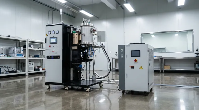
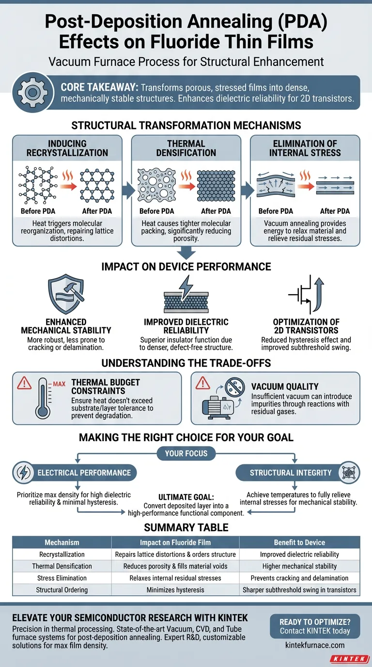
Post-deposition annealing (PDA) performed in a vacuum furnace is a critical thermal treatment designed to structurally enhance fluoride thin films through recrystallization and thermal densification. By applying controlled heat in a vacuum environment, this process significantly reduces the film's porosity and effectively eliminates internal residual stresses generated during the initial deposition.
Core Takeaway: The PDA process transforms fluoride thin films from a porous, stressed state into a dense, mechanically stable structure. This physical refinement directly enhances dielectric reliability, which is essential for minimizing hysteresis and improving the subthreshold swing in 2D transistor applications.
Structural Transformation Mechanisms
Inducing Recrystallization
The application of thermal energy during PDA allows the molecules within the fluoride film to reorganize. This triggers recrystallization, repairing lattice distortions and promoting a more ordered internal structure.
Thermal Densification
As the film is heated, the material undergoes densification, causing the molecules to pack more tightly together. This physical compaction significantly reduces porosity, removing voids that could otherwise compromise the material's integrity.
Elimination of Internal Stress
Deposition processes often leave the film with high levels of internal residual stress. Vacuum annealing provides the energy required to relax the material, effectively eliminating these stresses and preventing future structural failures.
Impact on Device Performance
Enhanced Mechanical Stability
By removing internal stresses and reducing porosity, the film becomes more robust. This mechanical stability ensures the film is less prone to physical defects such as cracking or delamination over time.
Improved Dielectric Reliability
The structural improvements translate directly to electrical performance. A denser, defect-free film offers superior dielectric reliability, functioning more effectively as an insulator in electronic components.
Optimization of 2D Transistors
For 2D transistors, the quality of the fluoride film is paramount. The PDA process contributes to a reduction in the hysteresis effect and an improvement in the subthreshold swing, leading to sharper, more efficient switching behavior.
Understanding the Trade-offs
Thermal Budget Constraints
While annealing improves film quality, it requires exposing the entire device to heat. You must ensure the thermal budget does not exceed the tolerance of the substrate or other underlying layers, which could lead to unwanted diffusion or degradation.
Vacuum Quality
The efficacy of this process relies heavily on the vacuum environment. If the vacuum pressure is insufficient, residual gases may react with the fluoride film during heating, potentially introducing new impurities rather than removing defects.
Making the Right Choice for Your Goal
To maximize the benefits of Post-Deposition Annealing, align the process parameters with your specific performance targets.
- If your primary focus is Electrical Performance: Prioritize annealing schedules that maximize density to ensure high dielectric reliability and minimal hysteresis in transistor operations.
- If your primary focus is Structural Integrity: Focus on achieving sufficient temperatures to fully relieve internal residual stresses, ensuring long-term mechanical stability.
The ultimate goal of vacuum PDA is to convert a deposited layer into a high-performance functional component through rigorous structural ordering.
Summary Table:
| Mechanism | Impact on Fluoride Film | Benefit to Device |
|---|---|---|
| Recrystallization | Repairs lattice distortions & orders structure | Improved dielectric reliability |
| Thermal Densification | Reduces porosity & fills material voids | Higher mechanical stability |
| Stress Elimination | Relaxes internal residual stresses | Prevents cracking and delamination |
| Structural Ordering | Minimizes hysteresis | Sharper subthreshold swing in transistors |
Elevate Your Semiconductor Research with KINTEK
Precision in thermal processing is the key to unlocking the full potential of fluoride thin films. KINTEK provides state-of-the-art Vacuum, CVD, and Tube furnace systems specifically engineered to handle the rigorous demands of post-deposition annealing.
Backed by expert R&D and world-class manufacturing, our customizable lab high-temp furnaces ensure precise temperature control and high-vacuum integrity, allowing you to achieve maximum film density and superior dielectric reliability for your 2D transistor applications.
Ready to optimize your thin film quality? Contact KINTEK today to discuss your unique project needs with our technical specialists.
Visual Guide
References
- Thin Fluoride Insulators for Improved 2D Transistors: From Deposition Methods to Recent Applications. DOI: 10.1002/pssr.202500200
This article is also based on technical information from Kintek Furnace Knowledge Base .
Related Products
- Vacuum Heat Treat Sintering and Brazing Furnace
- Small Vacuum Heat Treat and Tungsten Wire Sintering Furnace
- Vacuum Sealed Continuous Working Rotary Tube Furnace Rotating Tube Furnace
- Vacuum Heat Treat Sintering Furnace Molybdenum Wire Vacuum Sintering Furnace
- Vacuum Heat Treat Sintering Furnace with Pressure for Vacuum Sintering
People Also Ask
- What are the steps involved in a typical vacuum brazing treatment? Master the Process for Strong, Clean Joints
- What is the temperature of a vacuum furnace brazing? Optimize Your Joint Strength and Cleanliness
- What is the function of industrial vacuum heat treatment furnaces? Elevate 3D-Printed Maraging Steel Quality
- What are the benefits of using vacuum heat treating furnaces for metal alloys? Achieve Superior Metal Properties and Performance
- What are the technical advantages of using Ti-35Ni-25Nb foil? High toughness and beta-phase stability.


