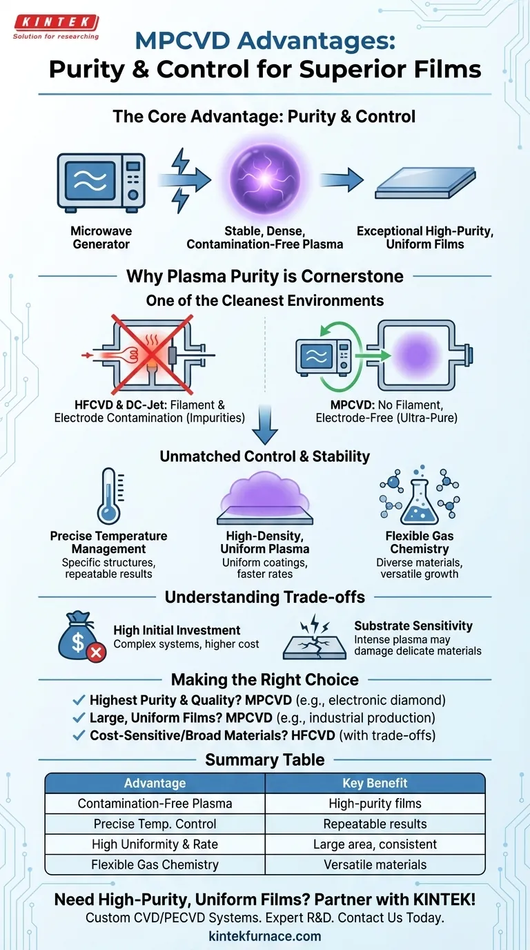
The primary advantages of MPCVD (Microwave Plasma Chemical Vapor Deposition) over other CVD methods are its ability to produce exceptionally high-purity films with precise control. By using microwave energy to generate a plasma, it eliminates common sources of contamination, like hot filaments, and creates a highly stable, uniform environment for material growth.
While many deposition techniques exist, MPCVD's core advantage lies in its unique method of plasma generation. Using clean microwave energy creates a stable, dense, and contamination-free reactive environment, which directly translates to superior film quality, uniformity, and purity for demanding applications.
Why Plasma Purity is the Cornerstone of MPCVD
The quality of a deposited film is fundamentally limited by the purity of the environment it grows in. MPCVD is engineered to create one of the cleanest possible deposition environments.
Eliminating Filament Contamination
In Hot Filament CVD (HFCVD), a metal wire is heated to high temperatures to decompose the precursor gases. This filament inevitably degrades over time, introducing metallic impurities into the film and compromising its properties.
MPCVD has no hot filament. The energy is delivered wirelessly via microwaves, removing this major source of contamination.
Electrode-Free Plasma
Some plasma systems, like DC-Jet CVD, use electrodes that are in direct contact with the plasma. These electrodes can sputter or erode, releasing particles that contaminate the film.
MPCVD is an electrodeless technique. The microwaves are coupled into the chamber from the outside, meaning the plasma itself is free of any physical components that could degrade and cause impurities.
Unmatched Control and Process Stability
Beyond purity, MPCVD provides a level of process control and stability that is difficult to achieve with other methods.
Precise Temperature Management
The system allows for stable and precise control over the reaction temperature. This is critical for achieving a specific crystal structure, controlling grain size, and ensuring repeatable results from run to run.
High-Density, Uniform Plasma
Microwave energy creates a high density of charged particles and reactive species. This dense plasma can be sustained over a large area, enabling the deposition of highly uniform films across large substrates.
Better homogeneity in the as-grown film is a direct result of this stable and widespread plasma environment. This also contributes to faster deposition rates compared to some thermal CVD methods.
Flexible Gas Chemistry
The clean, high-energy environment is compatible with a wide variety of precursor gases. This gives researchers and engineers the flexibility to experiment with different chemistries and deposit a broader range of materials.
Understanding the Trade-offs
No technology is perfect. Objectivity requires acknowledging MPCVD's limitations.
High Initial Investment
MPCVD systems are complex, requiring specialized microwave generators, waveguides, and vacuum chambers. This results in a significantly higher initial capital cost compared to simpler setups like HFCVD.
Substrate Sensitivity
The high-energy plasma, while beneficial for deposition, can be too harsh for certain delicate substrates. Materials like some polymers or organic compounds can be damaged by the intense microwave plasma, limiting the method's versatility for these specific applications.
Making the Right Choice for Your Goal
Selecting the correct deposition method depends entirely on your project's priorities.
- If your primary focus is the highest material purity and crystal quality (e.g., electronic-grade diamond): MPCVD is the definitive choice due to its contamination-free, stable plasma environment.
- If your primary focus is depositing large, highly uniform films for industrial production: MPCVD's ability to generate a large, stable plasma area provides unmatched consistency across the substrate.
- If your primary focus is cost-sensitive research or depositing on a wide variety of materials: A simpler method like HFCVD might be a pragmatic starting point, but you must accept the inherent trade-offs in film purity and quality.
Ultimately, selecting the right technique begins with understanding that MPCVD prioritizes film quality and control above all else.
Summary Table:
| Advantage | Key Benefit |
|---|---|
| Contamination-Free Plasma | No filament or electrode erosion, ensuring high-purity films. |
| Precise Temperature Control | Enables specific crystal structures and repeatable results. |
| High Uniformity & Deposition Rate | Dense plasma allows uniform coating across large substrates. |
| Flexible Gas Chemistry | Compatible with diverse precursors for versatile material growth. |
| Trade-offs | Higher initial cost; may damage delicate substrates. |
Need High-Purity, Uniform Films for Your Lab? Partner with KINTEK!
If your research or production demands the exceptional film quality and control offered by MPCVD technology, KINTEK is your ideal solution provider. Leveraging our deep expertise in R&D and in-house manufacturing, we deliver advanced high-temperature furnace solutions—including CVD/PECVD Systems—tailored to your unique requirements. Our strong customization capabilities ensure your system precisely matches your experimental goals, whether for electronic-grade diamond, large-area coatings, or specialized material growth.
Let’s elevate your deposition process. Contact our experts today to discuss your project and discover how KINTEK can empower your innovation!
Visual Guide
Related Products
- 915MHz MPCVD Diamond Machine Microwave Plasma Chemical Vapor Deposition System Reactor
- MPCVD Machine System Reactor Bell-jar Resonator for Lab and Diamond Growth
- Cylindrical Resonator MPCVD Machine System for Lab Diamond Growth
- Multi Heating Zones CVD Tube Furnace Machine for Chemical Vapor Deposition Equipment
- Inclined Rotary Plasma Enhanced Chemical Deposition PECVD Tube Furnace Machine
People Also Ask
- What factors influence the quality of diamond deposition in the MPCVD method? Master the Critical Parameters for High-Quality Diamond Growth
- What is the purpose of a microwave plasma chemical vapor deposition system? Grow High-Purity Diamonds and Advanced Materials
- What are the main components of an MPCVD machine? Unlock the Secrets of Diamond Synthesis
- What is the MPCVD method and why is it considered effective for diamond deposition? Superior Purity & High Growth Rates
- What are the essential components of an MPCVD reactor for diamond film deposition? Unlock High-Quality Diamond Growth


