Achieving optimal optical performance in plasmonic structures requires rigorous control over the deposition environment. High vacuum levels (approximately $10^{-8}$ mbar) and slow deposition rates are mandatory to guarantee the density, flatness, and adhesion of the gold layer. These parameters are critical for minimizing thermal stress and ensuring gold atoms uniformly fill lithographic masks, creating the precise geometries needed for surface plasmon resonance.
The structural integrity of gold nanocones—specifically their vertical sidewalls and material density—is directly dictated by the deposition environment. Without high vacuum and controlled rates, thermal stress and poor mask filling will compromise the resulting surface plasmonic properties.
The Physics of Deposition Quality
Ensuring Film Density and Flatness
To achieve a high-quality 400 nm gold layer, the environment must be devoid of interference. A high vacuum of $10^{-8}$ mbar minimizes the presence of background gases.
This lack of interference allows gold atoms to pack tightly. The result is a dense, flat film that supports the propagation of electromagnetic waves essential for plasmonics.
Maximizing Substrate Adhesion
Adhesion is often the failure point in metallization. A slow deposition rate allows gold atoms time to bond effectively with the substrate surface.
This controlled process prevents the film from peeling or flaking during subsequent processing steps.
Impact on Nanostructure Geometry
Controlling Thermal Stress
Electron-beam evaporation involves high energy, which translates to heat. If the deposition rate is too fast, the substrate heats up rapidly.
Maintaining a slow rate dissipates this energy. This minimizes thermal stress, preventing the gold or the underlying substrate from warping or cracking.
Uniform Mask Filling
For plasmonic applications, gold is often deposited into a polymer mask (such as PMMA) to form specific shapes like nanocones.
Slow rates ensure the gold fills these microscopic voids uniformly. This prevents gaps or voids that would ruin the optical response.
Achieving Vertical Sidewalls
The shape of the nanostructure defines its function. In this context, the goal is often truncated nanocones with vertical sidewalls.
Only a slow, constant rate ensures the metal builds up evenly along the mask walls. This geometric precision is required to tune the surface plasmonic properties accurately.
Common Pitfalls to Avoid
The Risk of Rushing the Rate
It is tempting to increase deposition rates to speed up fabrication. However, this introduces excessive kinetic energy and heat.
The immediate trade-off is structural deformation. The resulting thermal stress can distort the PMMA mask, leading to misshapen nanocones.
Vacuum Level Compromises
Operating at lower vacuum levels (higher pressure) introduces impurities. Residual gas molecules can become trapped in the film.
This reduces the purity and density of the gold. For plasmonic structures, this leads to dampening of the optical signal and poor performance.
Making the Right Choice for Your Goal
To maximize the performance of your plasmonic device, adhere to the following guidelines based on your specific priorities:
- If your primary focus is Geometric Precision: Prioritize a slow, constant deposition rate to ensure uniform filling of the PMMA mask and the formation of vertical sidewalls.
- If your primary focus is Film Durability: Maintain high vacuum ($10^{-8}$ mbar) to maximize film density and minimize the risk of delamination due to poor adhesion.
Precision in the deposition chamber translates directly to precision in optical performance.
Summary Table:
| Parameter | Targeted Level | Key Benefit for Plasmonics |
|---|---|---|
| Vacuum Pressure | ~10⁻⁸ mbar | Minimizes impurities; ensures high film density and flatness |
| Deposition Rate | Slow & Constant | Reduces thermal stress; enables uniform filling of PMMA masks |
| Film Quality | High Purity | Prevents damping of optical signals; ensures robust adhesion |
| Geometry | Vertical Sidewalls | Precise nanostructure shaping (e.g., nanocones) for resonance |
Elevate Your Thin Film Research with KINTEK
Achieving the geometric precision and material density required for advanced plasmonic structures starts with reliable hardware. KINTEK provides expert-engineered high-vacuum systems and evaporation solutions designed specifically for demanding R&D environments.
Backed by industry-leading manufacturing, our range of Vacuum, CVD, and customizable high-temperature lab systems ensures you have the control needed to minimize thermal stress and maximize film adhesion. Whether you are fabricating gold nanocones or complex semiconductor layers, KINTEK delivers the consistency your research demands.
Ready to optimize your deposition process? Contact our experts today to find the perfect customizable solution for your laboratory needs.
References
- Plasmonic‐Strain Engineering of Quantum Emitters in Hexagonal Boron Nitride. DOI: 10.1002/admi.202500071
This article is also based on technical information from Kintek Furnace Knowledge Base .
Related Products
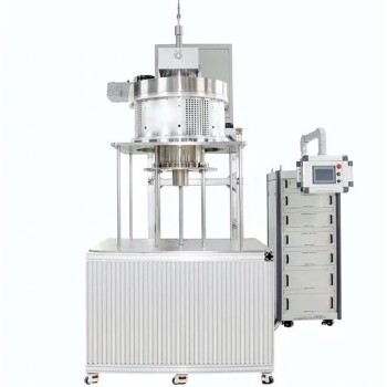
- 915MHz MPCVD Diamond Machine Microwave Plasma Chemical Vapor Deposition System Reactor
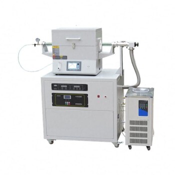
- Split Chamber CVD Tube Furnace with Vacuum Station CVD Machine
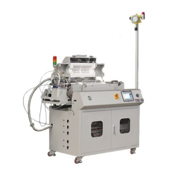
- Custom Made Versatile CVD Tube Furnace Chemical Vapor Deposition CVD Equipment Machine
- Multi Heating Zones CVD Tube Furnace Machine for Chemical Vapor Deposition Equipment
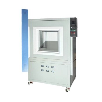
- High Temperature Muffle Oven Furnace for Laboratory Debinding and Pre Sintering
People Also Ask
- How does the ionization degree in MPCVD compare to other methods? Uncover Superior Film Quality and Speed
- What advantages does the Laser Chemical Vapor Deposition (LCVD) process offer? High Purity & Precision SiC Fibers
- What advantages do MPCVD diamond tools offer in industrial applications? Maximize Lifespan & Efficiency
- What are the key features of MPCVD single crystal diamond deposition equipment? Precision Control for High-Quality Growth
- What is Microwave Plasma Chemical Vapor Deposition (MPCVD)? Unlock Ultra-Pure Diamond Synthesis
