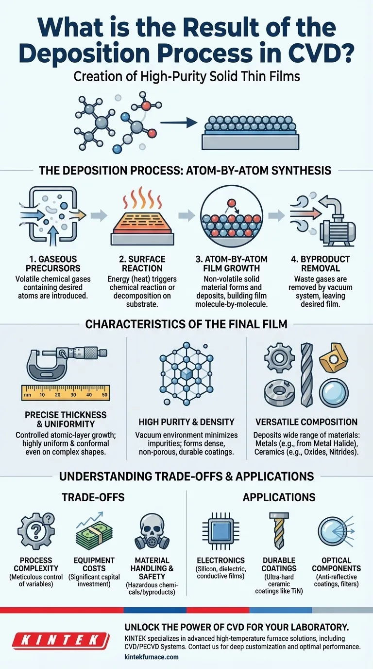
The result of the Chemical Vapor Deposition (CVD) process is the formation of a high-purity, solid thin film or coating on the surface of a substrate material. This new layer is built atom-by-atom or molecule-by-molecule from gaseous precursor chemicals that react or decompose, creating a durable and highly controlled material layer chemically bonded to the surface.
CVD is not simply about adding a layer; it is a precise engineering process for creating a functional, solid material with specific, controllable properties. The core result is a thin film whose quality, thickness, and chemical composition are meticulously determined by the process conditions.
How Deposition Fundamentally Works
The creation of a thin film via CVD is a controlled, multi-step process that transforms gas into a solid. It is fundamentally a process of synthesis directly on a surface.
The Role of Gaseous Precursors
The process begins with one or more volatile chemical gases, known as precursors, which contain the atoms you want to deposit. These gases are introduced into a vacuum chamber containing the object to be coated, called the substrate.
The Chemical Reaction on the Surface
Energy, typically in the form of high heat, is applied to the substrate. This energy causes the precursor gases to undergo a chemical reaction or to decompose directly on the hot surface of the substrate.
Atom-by-Atom Film Growth
This reaction leads to the formation of a new, non-volatile solid substance. This solid material deposits onto the substrate, building up a film molecule-by-molecule or atom-by-atom.
The Creation of Byproducts
The chemical reactions also produce other volatile gaseous substances, known as byproducts. These waste gases are removed from the chamber by the vacuum system, leaving only the desired solid film behind.
Characteristics of the Final Film
The result of this highly controlled process is a film with distinct and valuable characteristics that are difficult to achieve with other coating methods like painting or electroplating.
Precise Thickness and Uniformity
Because the film grows one atomic layer at a time, its thickness can be controlled with extreme precision, often down to the nanometer scale. The gaseous nature of the precursors allows them to reach all parts of a substrate, resulting in a highly uniform and conformal coating, even on complex shapes.
High Purity and Density
The vacuum environment minimizes the incorporation of impurities into the film. The chemical reaction process tends to form dense, non-porous coatings, resulting in a high-purity, durable material.
Versatile Material Composition
CVD is incredibly versatile. By choosing different precursor gases, you can deposit a wide range of materials. For example:
- Metals: A metal halide gas can decompose to form a pure metal film (
Metal Halide (g) → Metal (s) + Byproduct (g)). - Ceramics: A metal halide gas can be combined with an oxygen or nitrogen source to form a hard ceramic coating like an oxide or nitride.
Understanding the Trade-offs
While powerful, the precision of CVD comes with inherent complexities and considerations that are critical to understand.
Process Complexity
Achieving a high-quality film requires meticulous control over numerous variables. Temperature, pressure, gas flow rates, and precursor chemistry must be precisely managed, making process development a complex task.
Equipment Costs
CVD systems involve vacuum chambers, high-temperature heating elements, and sophisticated gas handling systems. This specialized equipment represents a significant capital investment.
Material Handling and Safety
Many precursor chemicals used in CVD are highly toxic, flammable, or corrosive. The process byproducts can also be hazardous, requiring strict safety protocols and exhaust management systems.
Applying CVD for Your Material Goal
The decision to use CVD is driven by the specific functional properties you need to engineer onto a surface.
- If your primary focus is creating highly pure electronic materials: CVD is the industry standard for depositing the silicon, dielectric, and conductive films that form the basis of microchips.
- If your primary focus is enhancing surface durability: CVD is used to apply ultra-hard ceramic coatings (like titanium nitride) to cutting tools, extending their life and improving performance.
- If your primary focus is fabricating advanced optical components: The precise thickness control offered by CVD is essential for creating anti-reflective coatings and complex optical filters.
Ultimately, understanding the result of CVD is understanding its power to engineer a material's surface from the atoms up.
Summary Table:
| Characteristic | Description |
|---|---|
| Film Formation | High-purity solid thin film or coating on substrate |
| Growth Process | Atom-by-atom or molecule-by-molecule from gaseous precursors |
| Key Properties | Precise thickness, uniformity, high purity, density, and versatile composition |
| Common Applications | Electronics, durable coatings, optical components |
Unlock the Power of CVD for Your Laboratory
At KINTEK, we specialize in delivering advanced high-temperature furnace solutions tailored to your unique needs. Leveraging exceptional R&D and in-house manufacturing, our product line—including Muffle, Tube, Rotary Furnaces, Vacuum & Atmosphere Furnaces, and CVD/PECVD Systems—ensures precise, reliable thin film deposition. Whether you're enhancing surface durability, fabricating electronic materials, or developing optical components, our strong deep customization capability guarantees optimal performance and efficiency.
Ready to elevate your research and production? Contact us today to discuss how KINTEK can support your goals with cutting-edge technology and expert solutions!
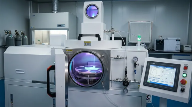
Visual Guide
Related Products
- Custom Made Versatile CVD Tube Furnace Chemical Vapor Deposition CVD Equipment Machine
- Multi Heating Zones CVD Tube Furnace Machine for Chemical Vapor Deposition Equipment
- HFCVD Machine System Equipment for Drawing Die Nano Diamond Coating
- 915MHz MPCVD Diamond Machine Microwave Plasma Chemical Vapor Deposition System Reactor
- RF PECVD System Radio Frequency Plasma Enhanced Chemical Vapor Deposition
People Also Ask
- What are the practical applications of gate media prepared by CVD tube furnaces? Unlock Advanced Electronics and More
- How does CVD tube furnace sintering enhance graphene growth? Achieve Superior Crystallinity and High Electron Mobility
- What are the key features of CVD tube furnaces for 2D material processing? Unlock Precision Synthesis for Superior Materials
- What temperature range do standard CVD tube furnaces operate at? Unlock Precision for Your Material Deposition
- Why are CVD tube furnace sintering systems indispensable for 2D material research and production? Unlock Atomic-Scale Precision


