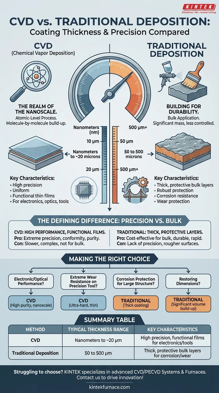
In a direct comparison, coatings produced by Chemical Vapor Deposition (CVD) are fundamentally thinner and more precise than those from traditional methods. CVD creates thin films measured in nanometers up to approximately 20 microns, whereas traditional deposition methods typically produce much thicker coatings, ranging from 50 to 500 microns.
The core difference is one of purpose. CVD is an atomic-level process designed for creating high-performance, functional thin films, while traditional methods are engineered for applying thick, protective bulk layers.
The Defining Difference: Precision vs. Bulk
Understanding the thickness disparity begins with understanding the radically different processes involved. Each method is a tool optimized for a very different scale and outcome.
Chemical Vapor Deposition (CVD): The Realm of the Nanoscale
CVD is a process where a substrate is exposed to volatile chemical precursors, which react or decompose on the surface to produce the desired thin film. This happens on a molecule-by-molecule basis.
This atomic-level control is why CVD excels at creating extremely thin, pure, and uniform coatings. The typical thickness ranges from just a few nanometers to just under 20 microns.
The primary advantage of CVD is not just thinness, but the precise control over the film's properties, such as its crystal structure, purity, and electrical characteristics.
Traditional Methods: Building for Durability
"Traditional methods" is a broad category that includes techniques like thermal spraying, electroplating, cladding, and even painting. These processes deposit material in a much less controlled, bulk fashion.
Their goal is often to apply a significant mass of material to a surface for robust protection or to build up worn areas. This results in coatings that are orders of magnitude thicker, typically ranging from 50 to 500 microns, and sometimes even more.
Here, the thickness itself is often the key feature, providing a sacrificial layer against corrosion or a substantial barrier against wear and abrasion.
Understanding the Trade-offs
Choosing a coating technology is about matching the process capabilities to the application's demands. There is no universally "better" method, only a more suitable one for a given problem.
The Limits of CVD
While highly precise, CVD is generally a more complex and slower process for building thickness. It is not practical or cost-effective for applications requiring a thick, bulk coating for general corrosion protection. Its strength is in function, not mass.
The Limits of Traditional Methods
These methods lack the precision, conformity, and purity of CVD. They cannot produce the ultra-thin, flawless layers required for semiconductor devices, advanced optics, or high-performance tool coatings where dimensional tolerance is critical. The resulting surfaces are also generally rougher.
Making the Right Choice for Your Application
Selecting the correct technology requires a clear understanding of your primary objective.
- If your primary focus is electronic or optical performance: CVD is the only choice for creating the necessary high-purity, nanometer-scale functional films.
- If your primary focus is extreme wear resistance on a precision tool: A thin, ultra-hard CVD coating provides the necessary surface properties without changing the part's critical dimensions.
- If your primary focus is corrosion protection for a large structure: A thick coating applied by a traditional method like thermal spray or painting offers the most cost-effective, long-term solution.
- If your primary focus is restoring dimensions on a worn component: A traditional build-up process is required to add the significant volume of material needed.
Ultimately, your decision hinges on whether your application demands the precise engineering of a functional surface or the robust application of a protective barrier.
Summary Table:
| Method | Typical Thickness Range | Key Characteristics |
|---|---|---|
| CVD (Chemical Vapor Deposition) | Nanometers to ~20 microns | High precision, uniform, functional thin films for electronics, optics, and tools |
| Traditional Deposition (e.g., thermal spraying, electroplating) | 50 to 500 microns | Thick, protective bulk layers for corrosion resistance and wear protection |
Struggling to choose the right coating method for your lab's unique needs? At KINTEK, we specialize in advanced high-temperature furnace solutions, including CVD/PECVD Systems, Muffle, Tube, and Rotary Furnaces, all backed by exceptional R&D and deep customization capabilities. Whether you require ultra-thin, precise coatings for electronics or durable layers for protection, our team can tailor a solution to enhance your experimental outcomes. Contact us today to discuss how we can support your specific application and drive innovation in your laboratory!
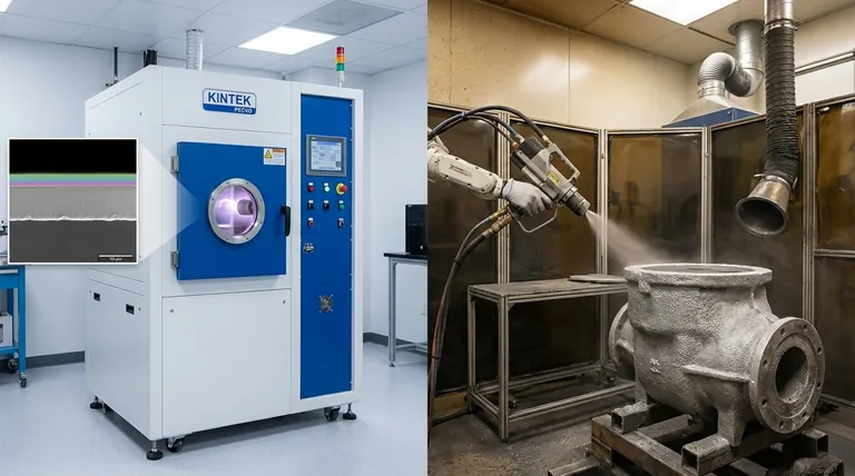
Visual Guide
Related Products
- HFCVD Machine System Equipment for Drawing Die Nano Diamond Coating
- Custom Made Versatile CVD Tube Furnace Chemical Vapor Deposition CVD Equipment Machine
- Multi Heating Zones CVD Tube Furnace Machine for Chemical Vapor Deposition Equipment
- RF PECVD System Radio Frequency Plasma Enhanced Chemical Vapor Deposition
- 915MHz MPCVD Diamond Machine Microwave Plasma Chemical Vapor Deposition System Reactor
People Also Ask
- What is the advantage of using a CVD system for coating turbine blades? Master Complex Geometries with Ease
- How can customers maximize the quality of CVD coatings? Master Pre-Coating Prep for Superior Results
- What materials are commonly used in CVD coating systems? Explore Key Materials for Superior Coatings
- What is the significance of the vacuum pressure control system in the CVD coating process for powders?
- What core function does CVD equipment serve in h-BN anti-corrosion? Master Precision Synthesis for High-Performance Films


