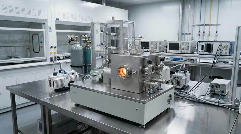
A Chemical Vapor Deposition (CVD) system is utilized to synthesize the critical active channel material for graphene-based field-effect transistors (FETs). Specifically, it is used to grow large-area, high-quality, single-layer single-crystal graphene on copper foil substrates through the high-temperature decomposition of methane gas.
Core Takeaway While there are various methods to produce graphene, CVD is essential for FET fabrication because it yields material with extremely low defect density and superior carrier mobility. These characteristics are required to ensure the transistor functions reliably and allows for the precise study of interface charge injection mechanisms.
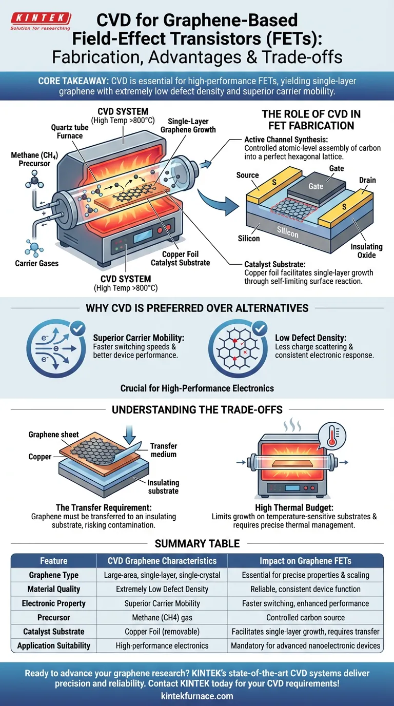
The Role of CVD in FET Fabrication
Creating the Active Channel
The core function of the CVD system in this context is to create the conductive "channel" of the transistor.
Unlike standard silicon processing, where the material is sliced from a boule, graphene must be synthesized atom-by-atom.
CVD provides the controlled environment necessary to assemble carbon atoms into a perfect hexagonal lattice.
The Precursor and Reaction
The process typically utilizes methane (CH4) as a gaseous precursor.
Inside the reaction chamber, the system applies high temperatures to thermally decompose the methane.
This decomposition releases carbon atoms, which then adsorb onto the surface of the substrate to form the graphene sheet.
The Role of the Catalyst Substrate
The primary reference specifies the use of copper foil as the substrate.
Copper acts as a catalyst that facilitates the surface reaction necessary for single-layer growth.
This self-limiting mechanism is crucial for FETs, as the electronic properties of single-layer graphene differ significantly from multi-layer stacks.
Why CVD is Preferred Over Alternatives
Superior Carrier Mobility
For a Field-Effect Transistor to function efficiently, charge carriers (electrons or holes) must move through the channel with minimal resistance.
Graphene produced via CVD exhibits superior carrier mobility compared to other methods.
This high mobility directly translates to faster switching speeds and better overall device performance.
Low Defect Density
Alternative methods, such as chemical reduction, often leave the carbon lattice riddled with imperfections.
CVD facilitates a highly ordered structure with extremely low defect density.
Fewer defects mean less scattering of charge carriers and a more consistent, predictable electronic response.
Understanding the Trade-offs
The Transfer Requirement
A major complexity in utilizing CVD for FETs is the substrate mismatch.
The graphene is grown on conductive copper foil, but a functioning FET requires the graphene to sit on an insulating substrate (like silicon dioxide).
Therefore, the CVD process is only the first step; the graphene must subsequently be transferred from the copper to the final device substrate, a process that can introduce contamination if not handled perfectly.
High Thermal Budget
CVD processes occur at high temperatures (often exceeding 800°C).
This requires specialized equipment capable of precise thermal management and gas flow delivery.
It also limits the ability to grow graphene directly onto temperature-sensitive substrates, reinforcing the need for the transfer process mentioned above.
Making the Right Choice for Your Goal
To determine if CVD is the right fabrication route for your specific application, consider the following:
- If your primary focus is high-performance electronics: CVD is the mandatory choice due to its ability to produce high-mobility, single-crystal graphene.
- If your primary focus is cost or scalable coatings: Lower-quality methods like chemical reduction may suffice, but they will not yield functioning high-speed transistors.
In summary, the CVD system is the foundational tool for enabling high-performance graphene electronics, trading process complexity for the pristine material quality required by FET devices.
Summary Table:
| Feature | CVD Graphene Characteristics | Impact on Graphene FETs |
|---|---|---|
| Graphene Type | Large-area, single-layer, single-crystal | Essential for precise electronic properties and device scaling |
| Material Quality | Extremely Low Defect Density | Minimizes charge scattering, ensures reliable and consistent device function |
| Electronic Property | Superior Carrier Mobility | Enables faster switching speeds and enhanced overall device performance |
| Precursor | Methane (CH4) gas | Controlled carbon source for atomic-level synthesis |
| Catalyst Substrate | Copper Foil (removable) | Facilitates single-layer growth; requires subsequent transfer to insulating substrate |
| Application Suitability | High-performance electronics | Mandatory for advanced, high-speed nanoelectronic devices and research |
Ready to advance your graphene research or FET fabrication? KINTEK’s state-of-the-art CVD systems are engineered for precision and reliability, producing the high-quality, low-defect graphene essential for cutting-edge nanoelectronics. Backed by expert R&D and manufacturing, KINTEK offers Muffle, Tube, Rotary, Vacuum, CVD systems, and other lab high-temp furnaces, all customizable for unique needs. Our solutions empower researchers and manufacturers to achieve superior material properties. Contact KINTEK today to discuss your specific CVD requirements and elevate your innovative projects! Reach out now
Visual Guide
References
- Kaili Zhang, Xiaoxiao Huang. Tracking Regulatory Mechanism of Trace Fe on Graphene Electromagnetic Wave Absorption. DOI: 10.1007/s40820-023-01280-6
This article is also based on technical information from Kintek Furnace Knowledge Base .
Related Products
- 915MHz MPCVD Diamond Machine Microwave Plasma Chemical Vapor Deposition System Reactor
- Custom Made Versatile CVD Tube Furnace Chemical Vapor Deposition CVD Equipment Machine
- RF PECVD System Radio Frequency Plasma Enhanced Chemical Vapor Deposition
- MPCVD Machine System Reactor Bell-jar Resonator for Lab and Diamond Growth
- HFCVD Machine System Equipment for Drawing Die Nano Diamond Coating
People Also Ask
- What are the main components of an MPCVD machine? Unlock the Secrets of Diamond Synthesis
- What factors influence the quality of diamond deposition in the MPCVD method? Master the Critical Parameters for High-Quality Diamond Growth
- How does the MPCVD process work to deposit diamond? A Guide to High-Purity Synthesis
- What are the essential components of an MPCVD reactor system? Build a Pristine Environment for High-Purity Materials
- In which industries is the microwave plasma chemical vapor deposition system commonly used? Unlock High-Purity Material Synthesis


