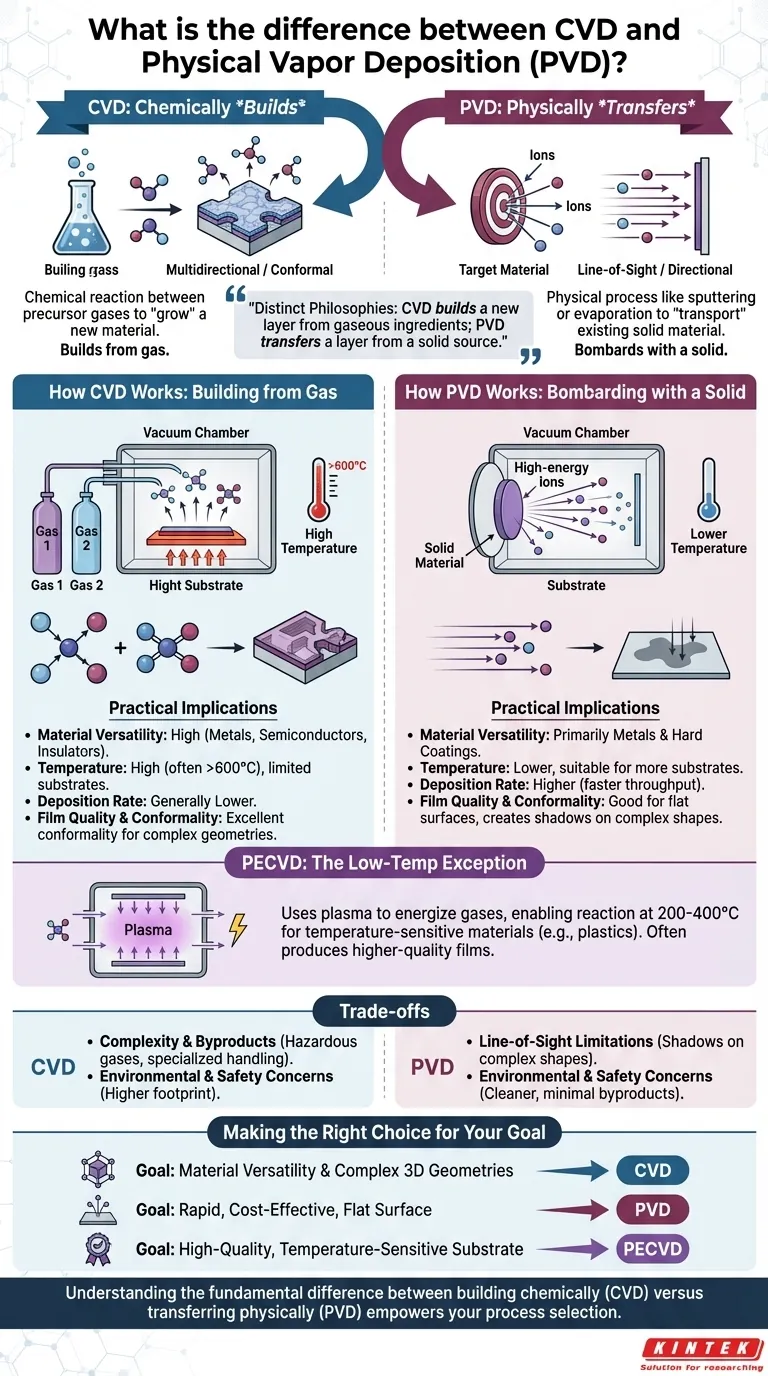
At its core, the difference between Chemical Vapor Deposition (CVD) and Physical Vapor Deposition (PVD) comes down to how the coating material arrives and forms on a surface. CVD uses a chemical reaction between precursor gases to "grow" a new material on the substrate, while PVD uses a physical process, like sputtering or evaporation, to "transport" an existing solid material onto the substrate.
The fundamental choice is not just between two acronyms, but between two distinct philosophies of film creation. CVD chemically builds a new layer from gaseous ingredients, while PVD physically transfers a layer from a solid source. This distinction dictates everything from material options to operating temperature and the geometry of what you can coat.
The Core Mechanism: Chemical Reaction vs. Physical Force
To select the right process, you must first understand their fundamentally different approaches to building a thin film.
How CVD Works: Building from Gas
In Chemical Vapor Deposition, precursor gases are introduced into a vacuum chamber containing the substrate.
Heat is applied to the substrate, triggering a chemical reaction among the gases on its surface. This reaction forms a solid film, effectively "growing" the desired material atom by atom.
Because the process is driven by the diffusion of gas, it is multidirectional. This allows CVD to create highly uniform and "conformal" coatings that cover complex, three-dimensional shapes without gaps or thin spots.
How PVD Works: Bombarding with a Solid
Physical Vapor Deposition begins with a solid source material, known as a "target."
This target is bombarded with high-energy ions inside a vacuum chamber, which physically dislodges or "sputters" atoms from the source. These vaporized atoms then travel through the chamber and deposit onto the substrate.
This process is a line-of-sight deposition. Atoms travel in a straight line from the target to the substrate, much like paint from a spray can. This makes it highly effective for flat surfaces but can create "shadows" on complex geometries.
Practical Implications for Your Project
The differences in their core mechanisms lead to significant practical consequences for temperature, material choice, and film quality.
Material Versatility
PVD is primarily used for depositing metals and some hard coatings like nitrides. Its strength lies in transferring pure materials with high efficiency.
CVD, by contrast, offers far greater versatility. By changing the precursor gases, it can deposit a vast range of materials, including metals, semiconductors (like silicon), and insulators (like silicon dioxide), making it indispensable in electronics manufacturing.
Temperature Requirements
Conventional CVD processes rely on high temperatures (often >600°C) to provide the thermal energy needed to drive the chemical reactions. This limits its use to substrates that can withstand extreme heat.
PVD generally operates at lower temperatures, making it suitable for a wider variety of substrates that might be damaged by the heat of traditional CVD.
The Key Exception: Plasma-Enhanced CVD (PECVD)
PECVD is a critical variant of CVD that overcomes the temperature limitation. Instead of relying solely on heat, it uses an electric field to generate a plasma.
This plasma energizes the precursor gases, allowing the chemical reaction to occur at much lower temperatures, typically 200-400°C. This opens the door for coating temperature-sensitive materials, such as plastics and assembled electronic devices.
Deposition Rate and Throughput
Generally, PVD processes offer a higher deposition rate than conventional CVD. This makes PVD a more attractive option for applications requiring thick films or high manufacturing throughput where speed is a priority.
Film Quality and Conformality
CVD's gas-based, multidirectional nature gives it a distinct advantage in conformality, or the ability to uniformly coat intricate topographies.
PECVD often produces higher-quality films than even conventional CVD, with reduced internal stress and a lower likelihood of cracking, making it ideal for demanding optical and electronic applications.
Understanding the Trade-offs
Neither method is universally superior. Your choice depends on navigating their inherent limitations.
CVD: Complexity and Byproducts
The primary drawback of CVD is its complexity. The process often involves toxic, corrosive, or flammable precursor gases that require specialized handling, safety protocols, and exhaust management systems.
PVD: Line-of-Sight Limitations
The key weakness of PVD is its directional nature. It is not well-suited for coating the inside of complex shapes, sharp corners, or deep trenches, as these areas will be "shadowed" from the source material.
Environmental and Safety Concerns
Due to the hazardous gases involved, CVD processes typically have a greater environmental and safety footprint than PVD. PVD is often considered a "cleaner" process with minimal hazardous byproducts.
Making the Right Choice for Your Goal
Your decision should be guided by the primary objective of your application.
- If your primary focus is material versatility or coating complex 3D geometries: CVD is the superior choice due to its ability to deposit non-metals and its excellent conformality.
- If your primary focus is rapid, cost-effective deposition of a simple metal film on a flat surface: PVD is often preferred for its high speed and operational simplicity.
- If your primary focus is depositing a high-quality film on a temperature-sensitive substrate like plastic: PECVD provides the ideal solution, combining the material versatility of CVD with a low-temperature process.
Ultimately, understanding the fundamental difference between building a film chemically (CVD) versus transferring it physically (PVD) empowers you to select the precise tool for your specific engineering challenge.
Summary Table:
| Aspect | CVD | PVD |
|---|---|---|
| Core Mechanism | Chemical reaction from gases | Physical transfer from solid target |
| Deposition Type | Multidirectional, conformal | Line-of-sight, directional |
| Temperature Range | High (often >600°C), lower with PECVD (200-400°C) | Generally lower |
| Material Versatility | High (metals, semiconductors, insulators) | Primarily metals and hard coatings |
| Ideal Applications | Complex 3D geometries, electronics | Flat surfaces, high throughput |
| Safety and Environment | Uses hazardous gases, higher footprint | Cleaner, minimal byproducts |
Struggling to choose between CVD and PVD for your lab? KINTEK specializes in advanced high-temperature furnace solutions, including CVD/PECVD Systems, Muffle, Tube, Rotary, Vacuum & Atmosphere Furnaces. With exceptional R&D and in-house manufacturing, we offer deep customization to precisely meet your unique experimental needs—ensuring optimal performance, efficiency, and safety. Let us help you select and customize the perfect system for your project. Contact us today to discuss your requirements!
Visual Guide
Related Products
- Custom Made Versatile CVD Tube Furnace Chemical Vapor Deposition CVD Equipment Machine
- Multi Heating Zones CVD Tube Furnace Machine for Chemical Vapor Deposition Equipment
- HFCVD Machine System Equipment for Drawing Die Nano Diamond Coating
- Split Chamber CVD Tube Furnace with Vacuum Station CVD Machine
- 915MHz MPCVD Diamond Machine Microwave Plasma Chemical Vapor Deposition System Reactor
People Also Ask
- What are the key application fields of CVD tube furnaces? Unlock Precision in Thin-Film Synthesis
- What improvements can be made to the bonding force of gate dielectric films using a CVD tube furnace? Enhance Adhesion for Reliable Devices
- Why are CVD tube furnace sintering systems indispensable for 2D material research and production? Unlock Atomic-Scale Precision
- What is a CVD tube furnace and what is its primary function? Discover Precision Thin-Film Deposition
- What temperature range do standard CVD tube furnaces operate at? Unlock Precision for Your Material Deposition