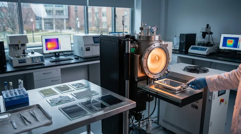
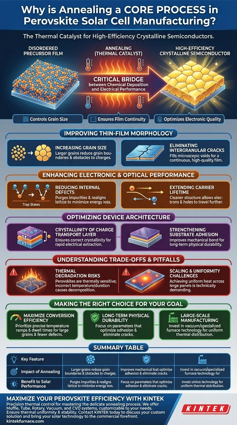
Annealing is the essential thermal catalyst that transforms a disordered precursor film into a high-efficiency crystalline semiconductor. It is considered a core process because it directly dictates the grain size, film continuity, and electronic quality of the perovskite layer. Without precise annealing, the resulting solar cell would suffer from poor charge transport and rapid degradation.
Annealing serves as the critical bridge between chemical deposition and electrical performance. By controlling the thermal environment, manufacturers can eliminate structural defects and optimize the light-harvesting properties of the perovskite film.
Improving Thin-Film Morphology
Increasing Grain Size
Annealing provides the energy necessary for crystal growth, leading to larger grain sizes within the perovskite structure. Larger grains are preferred because they reduce the total area of grain boundaries, which often act as obstacles to moving charges.
Eliminating Intergranular Cracks
The thermal process allows the material to settle and fill microscopic voids, effectively eliminating intergranular cracks. This creates a continuous, high-quality film that prevents electrical shunts and improves the overall structural integrity of the device.
Enhancing Electronic and Optical Performance
Reducing Internal Defects
Heat treatment helps purge impurities and realigns the atomic lattice to minimize internal defects. By reducing these "trap states," the cell can convert sunlight into electricity more efficiently with less energy loss.
Extending Carrier Lifetime
By creating a cleaner crystalline structure, annealing significantly extends the carrier lifetime. This allows electrons and "holes" to travel further through the material before recombining, which is a fundamental requirement for high-efficiency solar cells.
Optimizing Device Architecture
Crystallinity of the Charge Transport Layer
The impact of annealing extends beyond the perovskite layer itself to the charge transport layers. Proper thermal control ensures these layers have the correct crystallinity to facilitate the rapid movement of electricity out of the cell.
Strengthening Substrate Adhesion
Annealing improves the mechanical adhesion between the perovskite film and the underlying substrate. This bond is vital for the long-term physical durability of the solar panel, ensuring it can withstand environmental stressors.
Understanding the Trade-offs and Pitfalls
Thermal Degradation Risks
Perovskites are notoriously thermally sensitive compared to traditional silicon. If the annealing temperature is too high or the duration too long, the material can decompose, leading to a total loss of photovoltaic function.
Scaling and Uniformity Challenges
Achieving uniform temperature distribution across large-scale panels is technically demanding. Minor fluctuations in the thermal gradient can cause inconsistent grain sizes, leading to "hot spots" and reduced reliability in the final product.
Making the Right Choice for Your Goal
How to Apply This to Your Project
Proper annealing is a balancing act between achieving peak crystallinity and avoiding material decomposition.
- If your primary focus is Maximizing Conversion Efficiency: Prioritize precise temperature ramps and dwell times to maximize grain size and minimize electronic trap states.
- If your primary focus is Long-Term Physical Durability: Focus on the annealing parameters that optimize substrate adhesion and eliminate intergranular cracks to prevent moisture ingress.
- If your primary focus is Large-Scale Manufacturing: Invest in vacuum annealing or specialized furnace technology to ensure thermal uniformity across the entire surface area of the panel.
Mastering the annealing process is the single most important factor in transitioning perovskite research from the laboratory to a viable commercial product.
Summary Table:
| Key Feature | Impact of Annealing on Perovskite | Benefit to Solar Performance |
|---|---|---|
| Grain Size | Increases crystal size & reduces boundaries | Faster charge transport & higher efficiency |
| Film Morphology | Eliminates cracks and microscopic voids | Prevents shunts & improves structural integrity |
| Defect Density | Minimizes internal trap states | Reduces energy loss & extends carrier lifetime |
| Adhesion | Strengthens bond with substrate | Enhances long-term physical durability |
| Crystallinity | Optimizes charge transport layers | Facilitates rapid electrical extraction |
Maximize Your Perovskite Efficiency with KINTEK
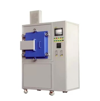
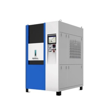
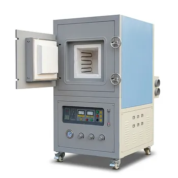
Precision thermal control is the difference between a failing film and a high-performance solar cell. KINTEK provides the specialized equipment needed to master the delicate annealing process. Backed by expert R&D and manufacturing, we offer Muffle, Tube, Rotary, Vacuum, and CVD systems, as well as other lab high-temp furnaces—all fully customizable to your unique research or production requirements.
Whether you are scaling up for manufacturing or optimizing light-harvesting properties in the lab, our systems ensure the thermal uniformity and stability your perovskite projects demand. Contact KINTEK today to discuss your custom solution and bring your solar technology to the commercial forefront.
Visual Guide
References
- Shengcong Wu, Peng Gao. Temperature Matters: Enhancing Performance and Stability of Perovskite Solar Cells through Advanced Annealing Methods. DOI: 10.3390/chemistry6010010
This article is also based on technical information from Kintek Furnace Knowledge Base .
Related Products
- Controlled Inert Nitrogen Hydrogen Atmosphere Furnace
- Spark Plasma Sintering SPS Furnace
- High Temperature Muffle Oven Furnace for Laboratory Debinding and Pre Sintering
- Vacuum Heat Treat Sintering Furnace with Pressure for Vacuum Sintering
People Also Ask
- How does hydrogen furnace annealing assist in preparing mechanically alloyed powders for compaction?
- How does atmospheric annealing in a controlled hydrogen furnace affect the cold compaction behavior of metal powders?
- What are the characteristics and uses of hydrogen atmosphere in furnaces? Achieve Superior Surface Purity and Bonding
- What are the characteristics and uses of hydrogen atmospheres in furnaces? Unlock Clean Metal Processing
- What controlled-atmosphere furnace conditions are required for sintering powder metallurgy copper alloy compacts? Ideal Setup