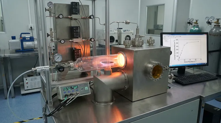
Diluted silane (SiH4) serves as the primary source for n-type silicon (Si) doping during the crystalline growth of beta-gallium oxide ($\beta$-Ga$_2$O$_3$). It acts as a gaseous precursor that introduces silicon atoms into the crystal lattice, enabling the material to conduct electricity by providing free electrons.
Core Takeaway: The precise regulation of diluted silane flow allows for exact control over silicon doping levels. This is the "knob" researchers turn to determine the material's free carrier concentration and electron mobility, effectively defining the electrical efficiency of the final power device.
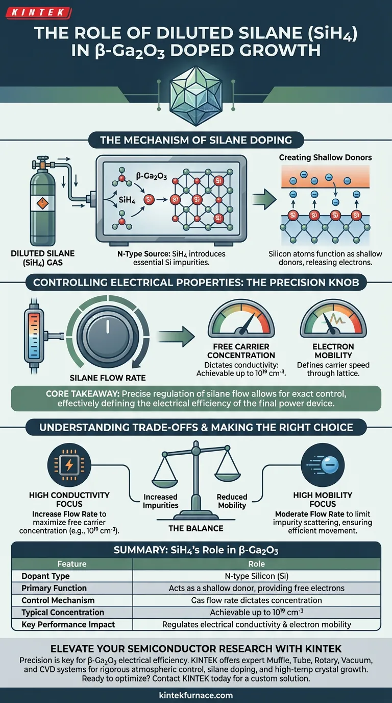
The Mechanism of Silane Doping
Acting as the N-Type Source
In the growth environment, diluted silane gas is introduced to provide the essential silicon (Si) impurities.
Without this introduction, beta-gallium oxide is typically highly insulating or unintentionally doped. The silane gas decomposes, releasing silicon atoms that incorporate themselves into the growing crystal structure.
Creating Shallow Donors
Once integrated into the lattice, these silicon atoms function as shallow donors.
This means they easily release electrons into the conduction band of the material. This release of electrons is what transforms the intrinsic beta-gallium oxide into an n-type semiconductor capable of carrying current.
Controlling Electrical Properties
Precision Through Flow Rate
The concentration of silicon in the final crystal is not random; it is dictated by the flow rate of the silane gas.
By strictly managing how much gas enters the chamber, researchers can achieve highly specific doping profiles. The primary reference notes that concentrations in the range of $10^{19} \text{ cm}^{-3}$ are achievable through this method.
Regulating Carrier Concentration and Mobility
The distribution of silicon directly determines two critical performance metrics: free carrier concentration and electron mobility.
Free carrier concentration defines how conductive the material is. Electron mobility defines how quickly those carriers can move through the lattice. Both factors are paramount for regulating the electrical performance of high-power devices.
Understanding the Trade-offs
The Balance of Conductivity and Quality
While introducing silane increases conductivity, it must be balanced carefully.
The primary goal is regulating electrical performance, not just maximizing it blindly. The concentration of silicon must be uniform and controlled to ensure the device operates reliably under power.
Impact on Mobility
There is an inherent relationship between doping concentration and electron mobility.
As the concentration of silicon dopants increases to boost conductivity, the electron mobility can be affected by the increased number of impurities. Precise control of the silane flow is the only way to optimize this balance for specific device requirements.
Making the Right Choice for Your Goal
To utilize diluted silane effectively in your growth process, consider your target device specifications:
- If your primary focus is high conductivity: Increase the silane flow rate to maximize the free carrier concentration, targeting levels such as $10^{19} \text{ cm}^{-3}$.
- If your primary focus is carrier mobility: Moderate the silane flow to limit impurity scattering, ensuring electrons can move efficiently through the lattice.
Success in beta-gallium oxide growth relies not just on introducing silane, but on the rigorous precision of its delivery.
Summary Table:
| Feature | Role of Silane (SiH4) in β-Ga2O3 Growth |
|---|---|
| Dopant Type | N-type Silicon (Si) |
| Primary Function | Acts as a shallow donor, providing free electrons |
| Control Mechanism | Gas flow rate dictates silicon concentration levels |
| Typical Concentration | Achievable up to $10^{19} \text{ cm}^{-3}$ |
| Key Performance Impact | Regulates electrical conductivity and electron mobility |
Elevate Your Semiconductor Research with KINTEK
Precision is the key to mastering the electrical efficiency of beta-gallium oxide. Backed by expert R&D and manufacturing, KINTEK offers specialized Muffle, Tube, Rotary, Vacuum, and CVD systems designed to provide the rigorous atmospheric control required for silane doping and high-temp crystal growth. Whether you are targeting high carrier mobility or peak conductivity, our customizable lab furnaces are built to meet your unique semiconductor fabrication needs.
Ready to optimize your doping profiles?
Contact KINTEK today for a custom solution
Visual Guide
References
- D. Gogova, Vanya Darakchieva. High crystalline quality homoepitaxial Si-doped <i>β</i>-Ga2O3(010) layers with reduced structural anisotropy grown by hot-wall MOCVD. DOI: 10.1116/6.0003424
This article is also based on technical information from Kintek Furnace Knowledge Base .
Related Products
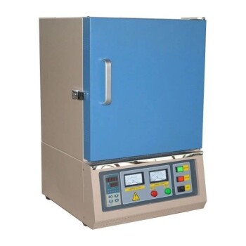
- 1200℃ Controlled Inert Nitrogen Atmosphere Furnace
- Small Vacuum Heat Treat and Tungsten Wire Sintering Furnace
- Multi Heating Zones CVD Tube Furnace Machine for Chemical Vapor Deposition Equipment
- Controlled Inert Nitrogen Hydrogen Atmosphere Furnace
- 1400℃ Muffle Oven Furnace for Laboratory
People Also Ask
- What are the key benefits of precise temperature control in a controlled atmosphere furnace? Unlock Superior Quality and Efficiency
- What factors should be considered when choosing a controlled atmosphere furnace? Ensure Optimal Performance for Your Materials
- How does a controlled atmosphere furnace prevent oxidation and decarburization? Master Precision Heat Treatment
- What types of gases are used in controlled atmosphere furnaces? Optimize Material Protection and Transformation
- What are the advantages of a controlled atmosphere furnace over tube furnaces? Superior Process Control for Sensitive Materials