At its core, Chemical Vapor Deposition (CVD) is a foundational manufacturing process used to create exceptionally thin, high-purity, high-performance solid films on a surface. It is the go-to method for industries that depend on materials with precisely engineered properties, from the semiconductor chips in your phone to the protective coatings on jet engine turbines and the biocompatible layers on medical implants.
CVD is not a single product but a versatile platform technology. Its true power lies in its ability to build materials layer by layer from a chemical gas, giving engineers unprecedented control over a material's purity, thickness, and structure at a near-atomic level.
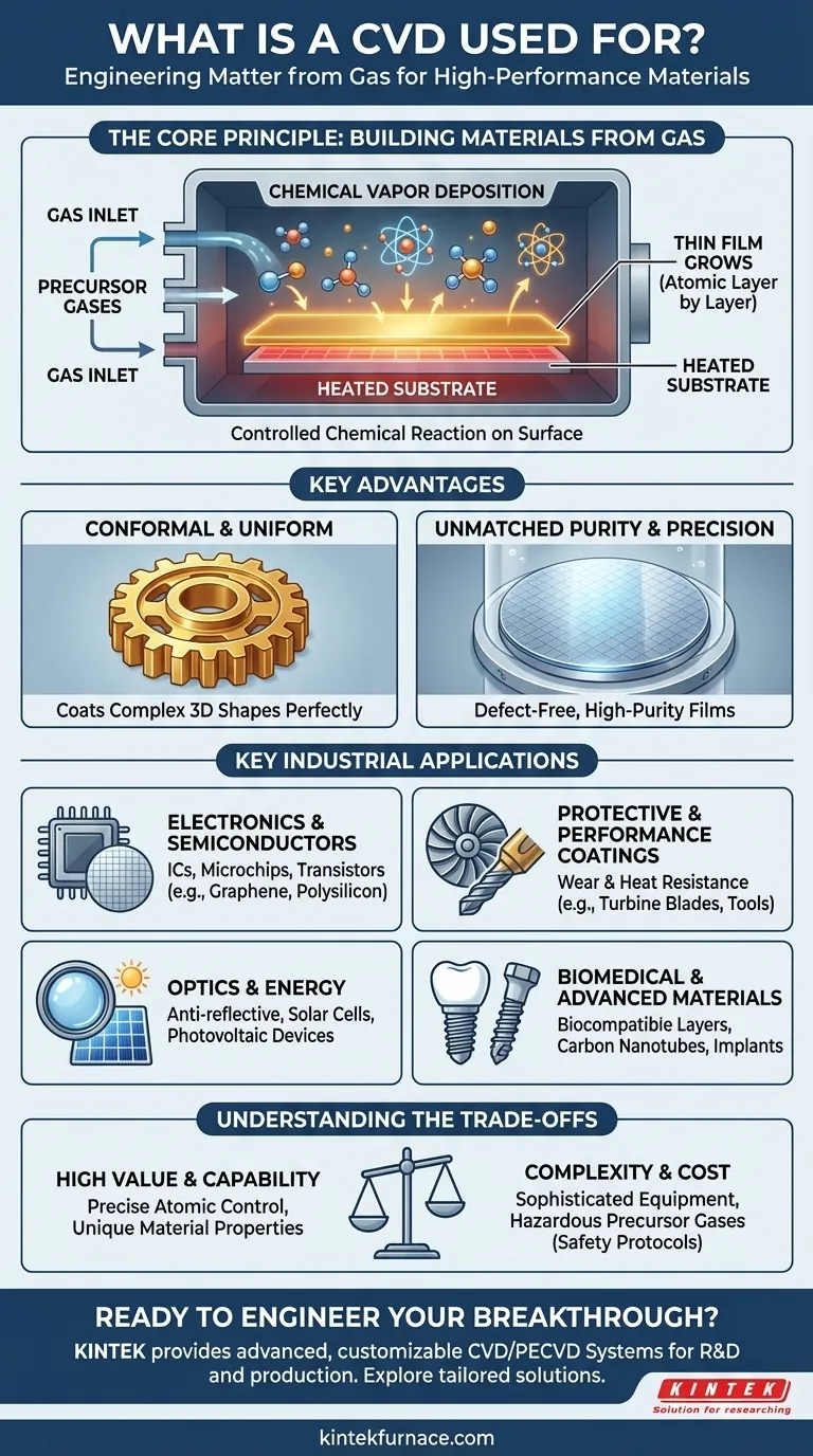
The Core Principle: Building Materials from Gas
CVD works by introducing reactive gases into a chamber containing the object to be coated, known as the substrate. These gases decompose and react on the heated substrate's surface, leaving behind a thin film of solid material.
A Controlled Chemical Reaction
Think of it as a highly controlled "spray painting" process, but instead of paint, you use specific gases. As these gases hit the hot surface, a chemical reaction is triggered, and a solid material "grows" directly onto the object, one atomic layer at a time.
Creating Conformal and Uniform Layers
A key advantage of CVD is its ability to produce conformal films. This means the deposited layer perfectly follows the contours of the substrate, evenly coating even the most complex and intricate 3D shapes. This is something traditional coating methods struggle to achieve.
Achieving Unmatched Purity and Precision
Because the process occurs in a vacuum-sealed chamber with highly pure gases, the resulting films are exceptionally pure and free of defects. This level of perfection is non-negotiable for applications like microelectronics.
Key Industrial Applications
The ability to create these perfect, thin films makes CVD indispensable across a vast range of high-tech industries.
Electronics and Semiconductors
This is the largest and most critical application. Modern electronics would not exist without CVD. It is used to deposit the multiple insulating, conductive, and semiconducting layers that form integrated circuits (ICs) and microchips.
Materials like silicon nitride, polysilicon, and advanced materials like graphene are deposited using CVD to build transistors and other microscopic components on silicon wafers.
Protective and Performance Coatings
CVD is used to drastically enhance the durability and performance of mechanical parts. A very hard material, like titanium nitride or diamond-like carbon, can be deposited onto cutting tools, bearings, or engine components to create an extremely wear-resistant surface.
In the aerospace industry, it's used to apply thermal barrier coatings to turbine blades, protecting them from the extreme heat inside a jet engine.
Optics and Energy
The process is vital for creating films with specific optical properties. This includes anti-reflective coatings on lenses and mirrors and creating the specialized layers within photovoltaic devices (solar cells) that convert light into electricity.
Biomedical and Advanced Materials
In the medical field, CVD applies ultra-thin, inert, and biocompatible coatings to implants like artificial joints and dental implants. This helps prevent the body from rejecting the implant and improves its longevity.
It is also used to fabricate advanced structures like carbon nanotubes and metal-organic frameworks (MOFs), which have unique properties for applications in drug delivery, water treatment membranes, and chemical sensing.
Understanding the Trade-offs
While powerful, CVD is not a universal solution. It involves specific complexities and limitations that make it suitable for high-value applications.
Equipment and Process Complexity
CVD systems are sophisticated and expensive. They require precise control over temperature, pressure, and the flow of precursor gases. Operating them requires significant expertise.
Chemical and Safety Constraints
The process is entirely dependent on the availability of suitable precursor gases that will react as desired at a given temperature. Many of these gases can be hazardous, toxic, or pyrophoric (igniting in air), requiring stringent safety protocols and handling infrastructure.
Making the Right Choice for Your Goal
Deciding if CVD is appropriate depends entirely on whether your goal requires the unique capabilities of atomic-level material control.
- If your primary focus is mass-produced electronics: CVD is the non-negotiable industry standard for fabricating the intricate layers of modern microprocessors and memory chips.
- If your primary focus is enhancing surface durability: CVD is a leading choice for applying high-performance wear, corrosion, or heat-resistant coatings to critical components where failure is not an option.
- If your primary focus is creating novel optical or medical devices: CVD enables the creation of highly specialized films, from biocompatible surfaces to layers with unique light-manipulating properties, that are often impossible to make any other way.
Ultimately, Chemical Vapor Deposition is a powerful tool for engineering matter at its most fundamental level, enabling the next generation of high-performance materials.
Summary Table:
| CVD Application Area | Key Materials Deposited | Primary Benefit |
|---|---|---|
| Electronics & Semiconductors | Silicon Nitride, Polysilicon, Graphene | Fabricates microscopic circuit components |
| Protective Coatings | Titanium Nitride, Diamond-Like Carbon | Provides extreme wear and heat resistance |
| Optics & Energy | Anti-reflective layers, Photovoltaic materials | Controls light absorption and reflection |
| Biomedical | Biocompatible coatings | Improves implant compatibility and longevity |
Ready to Engineer Your Next Breakthrough Material?
Leveraging exceptional R&D and in-house manufacturing, KINTEK provides diverse laboratories with advanced high-temperature furnace solutions, including our specialized CVD/PECVD Systems. Our strong deep customization capability allows us to precisely meet your unique experimental requirements for depositing high-purity, high-performance films.
Let's discuss how our technology can empower your research or production: Contact our experts today to explore a tailored solution
Visual Guide
Related Products
- Custom Made Versatile CVD Tube Furnace Chemical Vapor Deposition CVD Equipment Machine
- Multi Heating Zones CVD Tube Furnace Machine for Chemical Vapor Deposition Equipment
- HFCVD Machine System Equipment for Drawing Die Nano Diamond Coating
- Split Chamber CVD Tube Furnace with Vacuum Station CVD Machine
- 915MHz MPCVD Diamond Machine Microwave Plasma Chemical Vapor Deposition System Reactor
People Also Ask
- What improvements can be made to the bonding force of gate dielectric films using a CVD tube furnace? Enhance Adhesion for Reliable Devices
- Why are CVD tube furnace sintering systems indispensable for 2D material research and production? Unlock Atomic-Scale Precision
- What future trends are expected in the development of CVD tube furnaces? Discover Smarter, More Versatile Systems
- How does CVD tube furnace sintering enhance graphene growth? Achieve Superior Crystallinity and High Electron Mobility
- Which industries and research fields benefit from CVD tube furnace sintering systems for 2D materials? Unlock Next-Gen Tech Innovations


