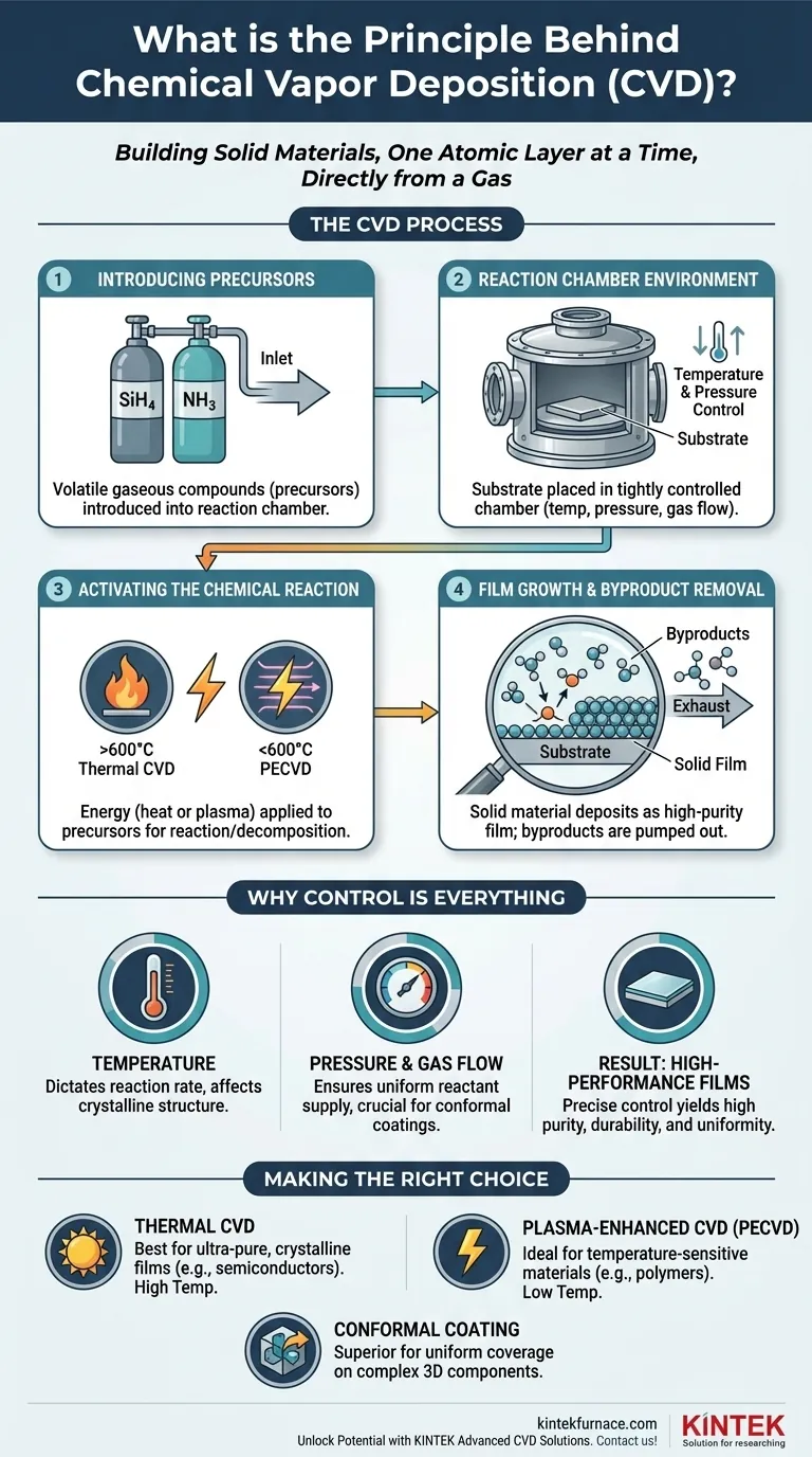
At its core, Chemical Vapor Deposition (CVD) is a process of building a solid material, one layer of atoms at a time, directly from a gas. It involves introducing specific gaseous molecules, known as precursors, into a reaction chamber. By applying energy—such as high heat or plasma—these gases react or decompose, and the resulting solid material deposits onto a target object (the substrate) as a high-purity, uniform thin film.
The fundamental principle of CVD is not merely coating a surface, but rather synthesizing a new solid material directly on it. It achieves this by using controlled chemical reactions in the vapor phase to transform volatile gases into a high-performance solid film with exceptional precision.
The CVD Process: From Gas to Solid Film
To truly understand CVD, we must look at it as a sequence of controlled physical and chemical events. Each step is critical for producing a high-quality final film.
Introducing the Precursors
The entire process begins with precursor gases. These are volatile compounds specifically chosen because they contain the chemical elements needed for the final film.
For example, to create a silicon nitride (Si₃N₄) film, one might use silane (SiH₄) and ammonia (NH₃) as precursors. These gases are precisely metered and transported into the reaction chamber.
The Reaction Chamber Environment
The substrate—the part to be coated—is placed inside a sealed reaction chamber. The conditions within this chamber, primarily temperature and pressure, are tightly controlled.
This controlled environment is essential for ensuring the chemical reactions happen exactly as intended, without interference from unwanted contaminants like oxygen or water vapor.
Activating the Chemical Reaction
This is the central step where the gas is transformed into a solid. Energy is applied to the precursor gases to give them the activation energy needed to react or decompose.
The method of energy delivery defines the type of CVD. For instance, Thermal CVD uses high temperatures (often >600°C), while Plasma-Enhanced CVD (PECVD) uses an electric field to create a plasma, allowing reactions to occur at much lower temperatures.
Film Growth and Byproduct Removal
As the precursors react on the hot substrate surface, the desired solid material "deposits" or grows, forming the thin film. Any unwanted gaseous byproducts from the reaction are continuously pumped out of the chamber.
This constant removal of byproducts is crucial for maintaining the purity of the growing film and driving the chemical reaction forward. The thickness of the film is precisely controlled by the deposition time and the concentration of the precursor gases.
Why Control Is Everything in CVD
The exceptional quality of CVD films—their purity, durability, and uniformity—is not an accident. It is the direct result of meticulous control over every process variable.
The Role of Temperature
Temperature is arguably the most critical parameter. It directly dictates the rate of the chemical reactions. Higher temperatures generally lead to faster deposition but can also influence the film's crystalline structure and internal stress.
Managing Pressure and Gas Flow
The chamber pressure and the flow rate of the gases determine the concentration of reactant molecules near the substrate. Precise control ensures that all parts of the substrate, even complex shapes, are exposed to a uniform supply of precursors.
This is why CVD is known for producing highly conformal coatings, meaning the film's thickness is perfectly uniform even over sharp corners and inside deep trenches.
The Result: High-Performance Films
By fine-tuning these variables, engineers can dictate the final properties of the film, including its thickness, density, chemical composition, and electrical characteristics. This level of control makes CVD an indispensable technology in advanced manufacturing.
Understanding the Trade-offs
While powerful, CVD is not a universal solution. Its effectiveness is balanced by significant practical considerations that are crucial for any technical evaluation.
High Temperature Requirements
Many traditional Thermal CVD processes require extremely high temperatures. This makes them unsuitable for coating temperature-sensitive materials, such as plastics or certain electronic components, which could be damaged or destroyed.
Precursor Handling and Safety
The precursor chemicals used in CVD can be highly toxic, flammable, or corrosive. Handling and disposing of these materials requires stringent safety protocols and specialized equipment, which adds to the operational complexity and cost.
Cost and Throughput
CVD systems are sophisticated and expensive pieces of equipment. The process can also be relatively slow compared to other coating methods like painting or electroplating, making it better suited for high-value applications rather than low-cost, bulk coating.
Making the Right Choice for Your Goal
Applying CVD effectively means matching the specific technique to your primary objective.
- If your primary focus is creating ultra-pure, crystalline films for semiconductors: Thermal CVD remains the benchmark due to its ability to produce films with the highest quality and lowest defect density.
- If your primary focus is coating temperature-sensitive materials like polymers or integrated circuits: Plasma-Enhanced CVD (PECVD) is the ideal choice because it enables deposition at much lower temperatures, preventing damage to the substrate.
- If your primary focus is achieving complete, uniform coverage on complex 3D components: The gas-phase nature of CVD makes it inherently superior to line-of-sight methods (like Physical Vapor Deposition) for creating conformal films.
Ultimately, mastering CVD is about harnessing controlled chemical reactions to build advanced materials with atomic-level precision.
Summary Table:
| Aspect | Description |
|---|---|
| Process | Gas-phase chemical reactions deposit solid films on substrates using precursors and energy activation. |
| Key Steps | 1. Introduce precursor gases. 2. Control chamber environment (temp, pressure). 3. Activate reaction (heat/plasma). 4. Grow film and remove byproducts. |
| Benefits | High purity, uniform conformal coatings, precise thickness control, and tailored film properties. |
| Common Types | Thermal CVD (high temp), Plasma-Enhanced CVD (PECVD, low temp). |
| Applications | Semiconductors, electronics, protective coatings, and advanced materials manufacturing. |
Unlock the potential of high-performance thin films for your laboratory with KINTEK's advanced CVD solutions. Leveraging exceptional R&D and in-house manufacturing, we provide diverse labs with tailored high-temperature furnace systems, including CVD/PECVD Systems, Muffle, Tube, Rotary, Vacuum & Atmosphere Furnaces. Our strong deep customization capability ensures precise alignment with your unique experimental needs, enhancing efficiency and results. Contact us today to discuss how we can support your innovation!
Visual Guide
Related Products
- 915MHz MPCVD Diamond Machine Microwave Plasma Chemical Vapor Deposition System Reactor
- Custom Made Versatile CVD Tube Furnace Chemical Vapor Deposition CVD Equipment Machine
- MPCVD Machine System Reactor Bell-jar Resonator for Lab and Diamond Growth
- HFCVD Machine System Equipment for Drawing Die Nano Diamond Coating
- RF PECVD System Radio Frequency Plasma Enhanced Chemical Vapor Deposition
People Also Ask
- What is the MPCVD method and why is it considered effective for diamond deposition? Superior Purity & High Growth Rates
- What are the essential components of an MPCVD reactor for diamond film deposition? Unlock High-Quality Diamond Growth
- What are some key features and benefits of the microwave plasma chemical vapor deposition system? Achieve Unmatched Material Synthesis
- What are the main components of an MPCVD machine? Unlock the Secrets of Diamond Synthesis
- What are the essential components of an MPCVD reactor system? Build a Pristine Environment for High-Purity Materials


