In short, Chemical Vapor Deposition (CVD) furnaces are critically important because they are the primary tool used to construct high-performance, ultra-thin films and coatings at an atomic level. This precision manufacturing is the bedrock of modern technology, enabling everything from the transistors in your smartphone to the durable coatings on jet engine turbines.
The core challenge in advanced manufacturing is controlling material properties with absolute precision. CVD furnaces solve this by allowing us to "grow" materials layer by layer from a chemical vapor, granting unparalleled control over purity, thickness, and structure, which in turn defines the performance of the final product.
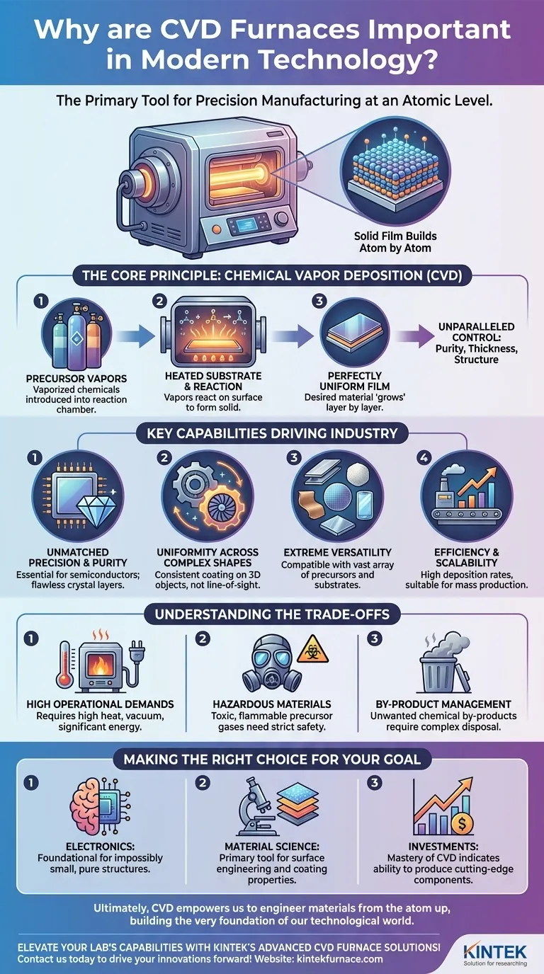
The Core Principle: Building Materials Atom by Atom
What is Chemical Vapor Deposition?
Chemical Vapor Deposition is a process for creating a solid, high-purity film on top of a surface, known as a substrate. It isn't a simple spray-on coating; it's more like 3D printing, but with individual atoms.
The process involves introducing one or more vaporized chemicals, called precursors, into a reaction chamber. When these vapors come into contact with the heated substrate inside the furnace, a chemical reaction is triggered.
This reaction causes a solid material to deposit, or "grow," onto the substrate, forming a perfectly uniform and thin film. Any excess chemicals or by-products are then exhausted from the chamber.
Why This Method is Transformative
The power of CVD lies in its controllability. By precisely adjusting factors like temperature, pressure, and the mix of precursor gases, engineers can dictate the exact properties of the film being created.
This includes its thickness (often measured in nanometers), chemical composition, crystal structure, and electrical properties. This level of control is simply not possible with most other deposition techniques.
Key Capabilities Driving Modern Industry
The unique nature of the CVD process provides several capabilities that make it indispensable for high-tech manufacturing.
Unmatched Precision and Purity
Because the film is built up from a chemical reaction, the resulting material can be exceptionally pure. This is non-negotiable for industries like semiconductors, where even the tiniest impurity can render a microchip useless.
CVD allows for the creation of flawless, single-crystal layers, which are the foundation of modern electronics.
Uniformity Across Complex Shapes
Unlike line-of-sight methods where a material is "sprayed," the gas in a CVD furnace flows around the substrate, coating it completely and evenly.
This means CVD can deposit a perfectly uniform film over complex, three-dimensional shapes, ensuring consistent performance across the entire surface of a component.
Extreme Versatility
The CVD process is compatible with a vast array of precursor chemicals and substrate materials.
This multifunctionality allows it to be used for depositing metals, ceramics, and polymers onto substrates ranging from silicon wafers to glass and metal alloys. This is why its applications are so broad, spanning dozens of industries.
Efficiency and Scalability
Compared to other high-precision techniques like Physical Vapor Deposition (PVD), CVD can often achieve higher deposition rates.
This efficiency, combined with its excellent repeatability, makes it highly suitable for mass production and is a key reason for its widespread industrial adoption.
Understanding the Trade-offs
While powerful, CVD technology is not without its challenges. Understanding these limitations is key to appreciating its role.
High Operational Demands
CVD processes often require very high temperatures and carefully controlled vacuum or pressure environments. This results in significant energy consumption and requires complex, expensive furnace systems.
Hazardous Materials
The precursor gases used in CVD can be toxic, flammable, or corrosive. This necessitates sophisticated safety protocols, gas handling systems, and exhaust treatment to protect workers and the environment.
By-Product Management
The chemical reactions that deposit the desired film also create unwanted by-products. These substances must be safely removed from the furnace and disposed of, adding a layer of complexity and cost to the overall process.
Making the Right Choice for Your Goal
Understanding the role of CVD is less about using it yourself and more about recognizing its impact on the technological landscape.
- If your primary focus is understanding modern electronics: Recognize that CVD is the foundational process for creating the impossibly small and pure layered structures that make up every transistor and microchip.
- If your primary focus is material science or engineering: View CVD as a primary tool for surface engineering, enabling you to enhance a material's properties with coatings that provide hardness, corrosion resistance, or specific optical/electrical functions.
- If your primary focus is evaluating technology investments: Consider a company's mastery of CVD processes as a key indicator of its ability to produce cutting-edge components for the semiconductor, aerospace, or renewable energy sectors.
Ultimately, Chemical Vapor Deposition empowers us to engineer materials from the atom up, building the very foundation of our technological world.
Summary Table:
| Aspect | Key Details |
|---|---|
| Core Principle | Builds solid films from vapor precursors via chemical reactions on heated substrates. |
| Key Capabilities | Unmatched precision, purity, uniformity on complex shapes, versatility, and scalability. |
| Common Applications | Semiconductors (transistors), aerospace coatings, renewable energy components. |
| Trade-offs | High temperatures, hazardous materials, by-product management, and operational costs. |
Elevate your lab's capabilities with KINTEK's advanced CVD furnace solutions! Leveraging exceptional R&D and in-house manufacturing, we provide high-temperature furnaces, including CVD/PECVD Systems, tailored for diverse laboratories. Our deep customization ensures precise alignment with your unique experimental needs, from semiconductor development to material science. Contact us today to discuss how our expertise can drive your innovations forward!
Visual Guide
Related Products
- Custom Made Versatile CVD Tube Furnace Chemical Vapor Deposition CVD Equipment Machine
- Split Chamber CVD Tube Furnace with Vacuum Station CVD Machine
- Multi Heating Zones CVD Tube Furnace Machine for Chemical Vapor Deposition Equipment
- Slide PECVD Tube Furnace with Liquid Gasifier PECVD Machine
- Controlled Inert Nitrogen Hydrogen Atmosphere Furnace
People Also Ask
- What are the key application fields of CVD tube furnaces? Unlock Precision in Thin-Film Synthesis
- Why are CVD tube furnace sintering systems indispensable for 2D material research and production? Unlock Atomic-Scale Precision
- What are the benefits of developing new precursor materials for CVD tube furnaces? Unlock Advanced Thin-Film Synthesis
- What future trends are expected in the development of CVD tube furnaces? Discover Smarter, More Versatile Systems
- How might AI and machine learning enhance CVD tube furnace processes? Boost Quality, Speed, and Safety


