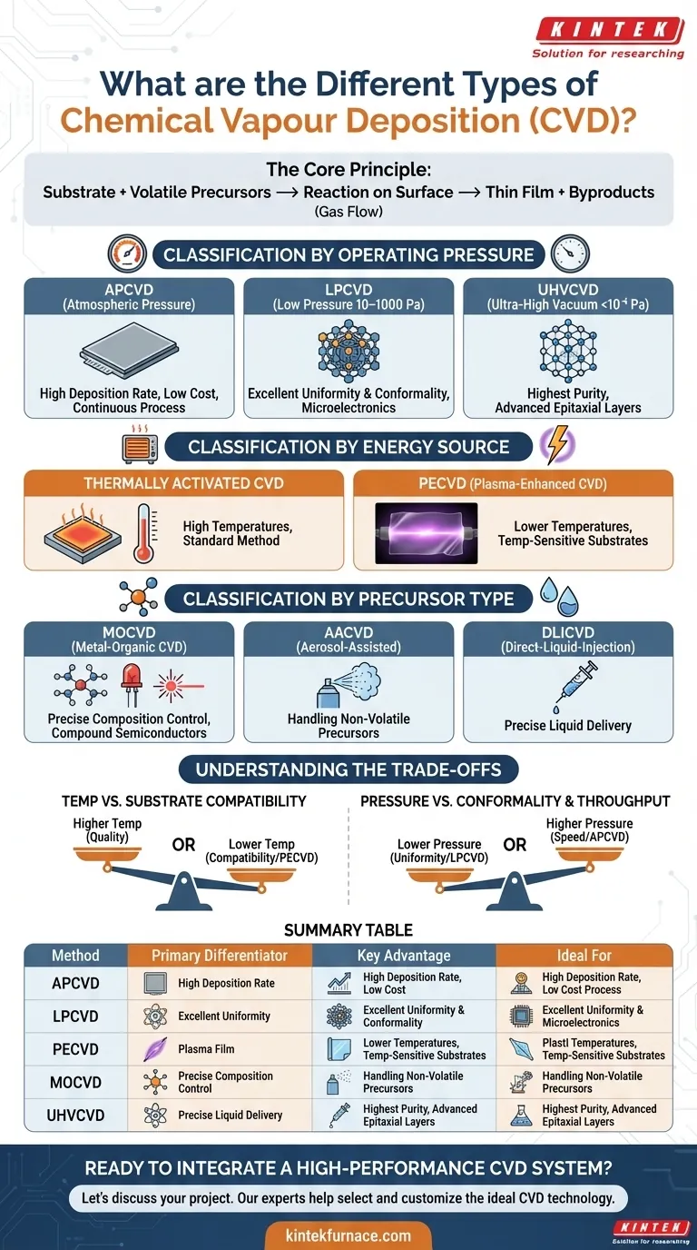
At its core, Chemical Vapor Deposition (CVD) is not a single technique but a family of processes used to create high-performance thin films and coatings. The different types of CVD are primarily classified based on their operating pressure, the energy source used to drive the reaction, and the physical state of the chemical precursors. Key variations include Atmospheric Pressure CVD (APCVD), Low-Pressure CVD (LPCVD), and Plasma-Enhanced CVD (PECVD), each optimized for different outcomes.
Understanding the various types of CVD is less about memorizing an alphabet soup of acronyms and more about grasping the fundamental trade-off: each method manipulates temperature, pressure, and energy to control the deposition of a specific material onto a substrate for a desired cost and quality.
The Core Principle of Deposition
What is CVD?
Chemical Vapor Deposition is a process where a substrate (the object to be coated) is exposed to one or more volatile chemical precursors. These precursors react or decompose on the substrate's surface to produce the desired thin film.
The excess chemical byproducts are then removed by a gas flow. Every type of CVD follows this basic sequence, but they differ in how they facilitate the chemical reaction.
Classification by Operating Pressure
The pressure inside the reaction chamber dramatically affects the deposition rate, film quality, and uniformity.
Atmospheric Pressure CVD (APCVD)
APCVD operates at normal atmospheric pressure. This simplicity allows for high deposition rates and a continuous process, making it cost-effective for large-scale production.
However, the high pressure can lead to gas-phase reactions, which can create particles and result in lower-quality, less uniform films.
Low-Pressure CVD (LPCVD)
LPCVD operates at a reduced pressure, typically in the range of 10–1000 Pa. This reduction minimizes unwanted gas-phase reactions and allows the precursor molecules to move more freely.
The result is films with excellent uniformity and conformality (the ability to coat complex, non-flat surfaces evenly). It is a foundational process in the manufacturing of microelectronics.
Ultra-High Vacuum CVD (UHVCVD)
Operating at extremely low pressures (below 10⁻⁶ Pa), UHVCVD is used when the highest possible film purity is required. The vacuum environment minimizes the incorporation of contaminants into the growing film.
This process is slower and more expensive, reserved for creating high-performance epitaxial layers in advanced semiconductor devices.
Classification by Energy Source
The chemical reactions in CVD require energy. The method used to supply this energy is another critical differentiator, especially for controlling deposition temperature.
Thermally Activated CVD
This is the most common form, where the substrate is heated to provide the thermal energy needed to decompose the precursors. Both APCVD and LPCVD are typically thermal CVD processes.
The primary limitation is that the substrate must be able to withstand high temperatures, often several hundred degrees Celsius.
Plasma-Enhanced CVD (PECVD)
PECVD uses an electric field to generate a plasma (an ionized gas). This highly reactive plasma provides the energy to break down precursor molecules at much lower temperatures than thermal CVD.
This makes PECVD essential for depositing films on temperature-sensitive substrates, such as polymers or pre-processed semiconductor wafers that cannot tolerate further high-heat cycles.
Classification by Precursor Type
Sometimes, CVD processes are defined by the specific type or delivery method of the chemical precursors.
Metal-Organic CVD (MOCVD)
MOCVD is a specialized form of thermal CVD that uses metal-organic compounds as precursors. These are organic molecules bonded to a metal atom.
This technique offers precise control over film composition and is critical for manufacturing compound semiconductors used in LEDs, lasers, and high-frequency electronics.
Aerosol-Assisted CVD (AACVD) and Direct-Liquid-Injection CVD (DLICVD)
These methods are designed to handle precursors that are not volatile enough to be easily turned into a gas.
In AACVD, the liquid precursor is atomized into a fine aerosol and carried into the chamber by a gas. In DLICVD, a precise amount of liquid precursor is injected directly into a heated vaporization zone. Both techniques expand the range of materials that can be deposited via CVD.
Understanding the Trade-offs
There is no single "best" type of CVD. The choice is always a matter of balancing competing requirements.
Temperature vs. Substrate Compatibility
Higher temperatures often produce more crystalline, higher-quality films. However, they can damage or warp the underlying substrate. This is the central problem that PECVD was designed to solve, enabling deposition on plastics and other sensitive materials.
Pressure vs. Conformality and Throughput
Lower pressures, as in LPCVD, are unmatched for creating uniform and conformal coatings over complex 3D structures. However, this is typically a slower, batch process. Higher-pressure APCVD sacrifices some quality for speed and continuous throughput, making it ideal for simpler, large-area coatings.
Cost vs. Performance
A simple thermal APCVD reactor लाइन is relatively inexpensive to build and operate. In contrast, MOCVD, PECVD, and UHVCVD systems are significantly more complex and expensive, justified only by the need for the high-performance films they produce.
Choosing the Right CVD Method
Your choice of CVD technique should be guided by your end goal, substrate material, and production scale.
- If your primary focus is low-cost, large-area coating: APCVD is often the most economical choice due to its high deposition rate and simpler equipment.
- If your primary focus is excellent film uniformity on complex surfaces: LPCVD is the industry standard for applications like integrated circuits and MEMS.
- If your primary focus is depositing films on temperature-sensitive materials: PECVD is the necessary choice to avoid damaging your substrate.
- If your primary focus is creating ultra-pure, crystalline layers for high-end electronics: MOCVD or UHVCVD are the specialized, high-performance tools for the job.
By understanding these distinct methods as a set of tools, you can intentionally select the process that best balances performance, material compatibility, and cost for your specific application.
Summary Table:
| CVD Method | Primary Differentiator | Key Advantage | Ideal For |
|---|---|---|---|
| APCVD | Atmospheric Pressure | High deposition rate, low cost | Large-area, simple coatings |
| LPCVD | Low Pressure | Excellent uniformity & conformality | Microelectronics, MEMS |
| PECVD | Plasma Energy Source | Low-temperature deposition | Temperature-sensitive substrates (e.g., polymers) |
| MOCVD | Metal-Organic Precursors | Precise composition control | Compound semiconductors (LEDs, lasers) |
| UHVCVD | Ultra-High Vacuum | Highest film purity | Advanced semiconductor epitaxy |
Ready to Integrate a High-Performance CVD System into Your Lab?
Navigating the complexities of Chemical Vapor Deposition to find the perfect process for your specific material and substrate requirements is a significant challenge. KINTEK is here to turn that challenge into a success.
Leveraging our exceptional R&D and in-house manufacturing capabilities, we provide diverse laboratories with advanced high-temperature furnace solutions, including specialized CVD and PECVD Systems. Our strong deep customization capability allows us to precisely tailor systems to meet your unique experimental and production needs, whether you require the high throughput of APCVD or the precision of UHVCVD.
Let's discuss your project. Our experts will help you select and customize the ideal CVD technology to achieve superior thin films, enhance your research outcomes, and optimize your production scale.
➡️ Contact KINTEK today to schedule a consultation
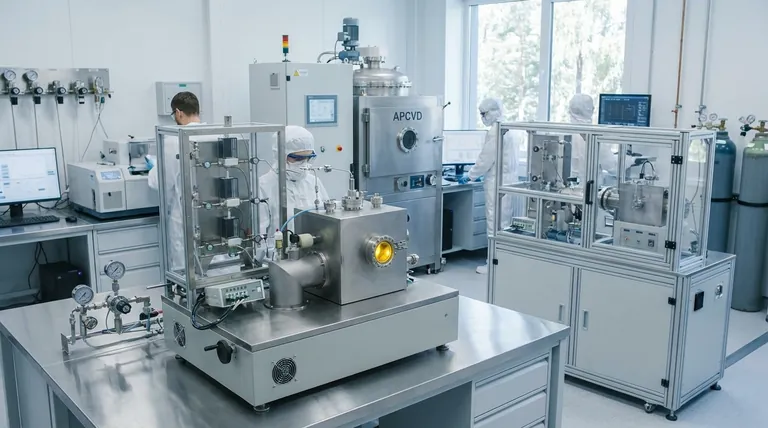
Visual Guide
Related Products
- Custom Made Versatile CVD Tube Furnace Chemical Vapor Deposition CVD Equipment Machine
- MPCVD Machine System Reactor Bell-jar Resonator for Lab and Diamond Growth
- Multi Heating Zones CVD Tube Furnace Machine for Chemical Vapor Deposition Equipment
- 915MHz MPCVD Diamond Machine Microwave Plasma Chemical Vapor Deposition System Reactor
- Slide PECVD Tube Furnace with Liquid Gasifier PECVD Machine
People Also Ask
- What are the benefits of developing new precursor materials for CVD tube furnaces? Unlock Advanced Thin-Film Synthesis
- What customization options are available for CVD tube furnaces? Tailor Your System for Superior Material Synthesis
- What temperature range do standard CVD tube furnaces operate at? Unlock Precision for Your Material Deposition
- What are the key features of CVD tube furnaces for 2D material processing? Unlock Precision Synthesis for Superior Materials
- How might AI and machine learning enhance CVD tube furnace processes? Boost Quality, Speed, and Safety


