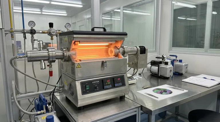
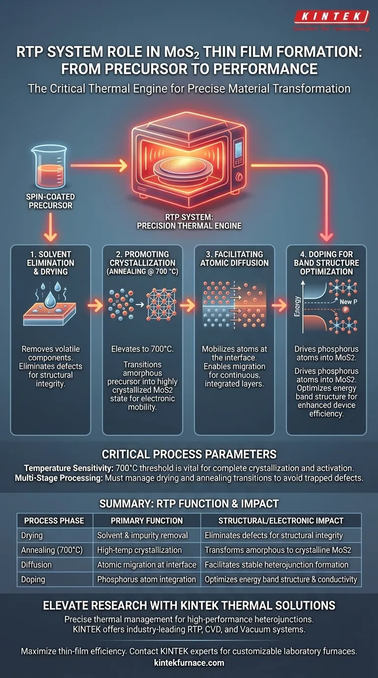
A Rapid Thermal Processing (RTP) system functions as the critical thermal engine for transforming raw precursors into functional Molybdenum Disulfide (MoS2) thin films. By subjecting spin-coated layers to precise high-temperature annealing—typically at 700 °C—the RTP system drives the essential phase changes required for device performance. It is responsible for simultaneously crystallizing the material, removing impurities, and facilitating atomic doping to tune electronic properties.
The RTP system is not merely a heater; it is a precision tool that orchestrates the crystallization of MoS2 while simultaneously driving atomic diffusion for doping. This dual action optimizes the material's energy band structure, making it essential for creating high-performance heterojunctions.
The Mechanics of Film Transformation
To understand the value of the RTP system, one must look beyond simple heating and understand how it physically alters the material structure at the atomic level.
Solvent Elimination and Drying
The initial function of the RTP system is purification. Before high-quality films can form, the system dries the spin-coated precursor to remove volatile components. This step eliminates residual solvents that, if left behind, would create defects and degrade the structural integrity of the final film.
Promoting Crystallization
The core value of the RTP process lies in its high-temperature annealing capabilities. By elevating the temperature to approximately 700 °C, the system provides the thermal energy required to reorder the atomic structure. This promotes the transition of the amorphous precursor into a highly crystallized MoS2 state, which is a prerequisite for superior electronic mobility.
Interface Engineering and Doping
Beyond structural formation, the RTP system plays an active role in defining the electronic characteristics of the MoS2 film through atomic manipulation.
Facilitating Atomic Diffusion
The high thermal energy generated by the RTP system does more than just settle the MoS2 lattice; it mobilizes atoms at the interface. The process facilitates atomic diffusion, allowing specific elements to migrate into the film structure. This controlled movement is vital for creating integrated, continuous interfaces between different material layers.
Doping for Band Structure Optimization
Specifically, the RTP process drives phosphorus atoms into the MoS2 to form a doped layer. This is not an accidental byproduct but a targeted outcome of the thermal treatment. By introducing these dopants, the process optimizes the energy band structure of the heterojunction, directly enhancing the device's electrical efficiency and performance.
Critical Process Parameters
While the RTP system is a powerful tool for synthesis, its effectiveness relies on strict adherence to process parameters.
Temperature Sensitivity
The specific target of 700 °C is not arbitrary; it represents a critical threshold for this reaction. Failing to reach this temperature may result in incomplete crystallization or insufficient activation of the dopants. Conversely, excessive heat could lead to material degradation or uncontrolled diffusion that blurs the heterojunction interface.
The Necessity of Multi-Stage Processing
The RTP must handle two distinct phases: the initial drying and the subsequent high-temperature annealing. Attempting to rush the transition between drying (solvent removal) and annealing (crystallization) can trap defects within the lattice. The system must effectively manage both regimes to ensure a high-quality final layer.
Making the Right Choice for Your Goal
The RTP system acts as the bridge between a raw chemical precursor and a functional electronic component. Your specific objectives will dictate which aspect of the RTP process requires the most attention.
- If your primary focus is Structural Integrity: Prioritize the drying and solvent removal phases to ensure the precursor is contaminant-free before high-temperature crystallization begins.
- If your primary focus is Electronic Performance: Focus on the precision of the 700 °C annealing step to maximize phosphorus doping and optimize the energy band alignment.
The RTP system is the defining instrument for converting potential chemical properties into realized electronic performance through precise thermal control.
Summary Table:
| Process Phase | Primary Function | Structural/Electronic Impact |
|---|---|---|
| Drying | Solvent & impurity removal | Eliminates defects for structural integrity |
| Annealing (700°C) | High-temp crystallization | Transforms amorphous layers to crystalline MoS2 |
| Diffusion | Atomic migration at interface | Facilitates stable heterojunction formation |
| Doping | Phosphorus atom integration | Optimizes energy band structure & conductivity |
Elevate Your Semiconductor Research with KINTEK
Precise thermal management is the difference between a defective layer and a high-performance heterojunction. KINTEK provides industry-leading thermal solutions, including RTP, CVD, and Vacuum systems, engineered specifically for the rigorous demands of material synthesis and atomic doping.
Whether you are refining MoS2 crystallization or developing complex thin-film stacks, our customizable laboratory furnaces offer the temperature uniformity and rapid response required for repeatable excellence.
Maximize your thin-film efficiency—contact KINTEK experts today to find the perfect thermal system for your research goals.
Visual Guide
References
- Sel Gi Ryu, Keunjoo Kim. Photoenhanced Galvanic Effect on Carrier Collection of the MOS<sub>2</sub> Contact Layer in Silicon Solar Cells. DOI: 10.1002/pssa.202500039
This article is also based on technical information from Kintek Furnace Knowledge Base .
Related Products
- Laboratory Quartz Tube Furnace RTP Heating Tubular Furnace
- RF PECVD System Radio Frequency Plasma Enhanced Chemical Vapor Deposition
- Split Multi Heating Zone Rotary Tube Furnace Rotating Tube Furnace
- Inclined Rotary Plasma Enhanced Chemical Deposition PECVD Tube Furnace Machine
- Vacuum Heat Treat Furnace with Ceramic Fiber Liner
People Also Ask
- What physical conditions does a laboratory Tube Furnace provide for SOEC? Precision Heat for Solid Oxide Characterization
- What are the main features and functions of a laboratory tube furnace? Unlock Precise High-Temp Control for Your Lab
- What conditions do tube furnaces provide for Au-Seeded TiO2 nanowires? Master Precision Thermal Synthesis
- What role does a laboratory tube furnace system play in the catalytic pyrolysis of LLDPE? Enhancing Yield and Precision
- What conditions does a tube furnace provide for post-ion-implantation? Achieve Precise Microstructural Repair


