At its core, chemical vapor deposition (CVD) is a highly precise manufacturing process used to create high-performance, ultra-thin solid films. It is the foundational technology behind the modern semiconductor industry and is essential for producing a wide range of electronic components, including sensors, microchips, and advanced optical coatings for consumer and industrial products.
CVD is not merely a coating technique; it is an atomic-level construction method. It allows engineers to build materials from the ground up, molecule by molecule, to achieve specific properties like extreme hardness, electrical conductivity, or chemical resistance that are impossible to attain with conventional methods.
How CVD Enables Modern Technology
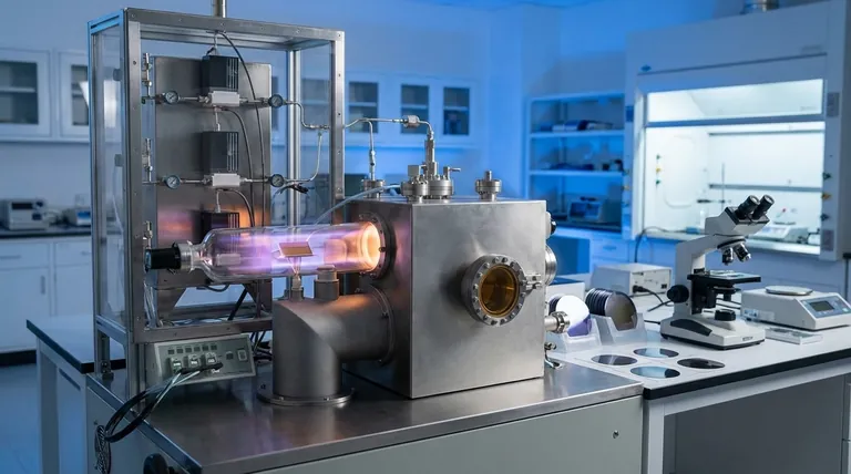
To understand why CVD is so widely used, you must first understand its fundamental process. It isn't a spray or a dip; it is a meticulously controlled reaction inside a vacuum chamber.
The Process: Building Atom by Atom
The CVD process involves introducing one or more volatile precursor gases into a vacuum chamber containing the object to be coated, known as the substrate. When these gases come into contact with the heated substrate, they react or decompose, depositing a solid material directly onto the surface. This happens one layer of atoms or molecules at a time, creating a perfectly uniform and dense film.
The Result: High-Purity, High-Performance Films
Because the deposition is so controlled, the resulting films are exceptionally pure, dense, and free of defects. This quality is what makes CVD essential for applications where material performance is critical. The process creates a durable, dry coating that is chemically bonded to the substrate without any need for curing.
A Foundation for the Semiconductor Industry
Modern microelectronics would not exist without CVD. The microscopic circuits on a computer chip require incredibly thin layers of conducting, insulating, and semiconducting materials. CVD is the only process with the precision to deposit these films reliably at the nanometer scale required for today's advanced processors and memory chips.
Creating Advanced Materials
CVD is also used to synthesize materials with extraordinary properties. For example, specific CVD processes can grow films of pure, polycrystalline diamond, one of the hardest materials known. This is used for durable coatings on industrial tools, high-performance optics, and even in the gem industry. Other variations can produce carbon nanotubes and nanowires, materials with unique electrical and mechanical properties that are central to next-generation electronics and medical devices.
Key Application Areas in Detail
CVD's versatility makes it a critical process across numerous high-tech industries.
Electronics and Sensors
From the smartphone in your pocket to the safety systems in your car, CVD is everywhere. It is used to produce the thin films in automotive sensors, HVAC sensors, smart home devices, wearables, and medical biosensors. The stability and reliability of these CVD-created films are what make the devices accurate and long-lasting.
Optics and Electrochemistry
The ability to control a film's thickness and purity allows engineers to create specialized optical coatings. These layers can enhance light transmission, create reflective surfaces, or protect lenses from scratching. In electrochemistry, CVD films serve as durable electrodes or protective barriers against corrosion.
Understanding the Trade-offs
While powerful, CVD is not the solution for every application. Its precision comes with specific challenges that make it unsuitable for some use cases.
Complexity and Cost
CVD systems are complex machines that require vacuum chambers, precise gas handling, and high-temperature controls. This makes the initial investment and operating costs significantly higher than simpler coating methods.
Handling of Precursor Materials
The precursor gases used in CVD can be highly toxic, flammable, or corrosive. Safely managing these materials requires strict safety protocols and specialized facility infrastructure, adding to the overall operational complexity.
Slower Deposition Rates
Building a film atom by atom is inherently slower than bulk coating methods like painting or electroplating. For applications where ultimate precision and purity are less important than speed and volume, other methods are often more economical.
Making the Right Choice for Your Goal
Selecting a manufacturing process depends entirely on your performance requirements and economic constraints.
- If your primary focus is ultimate performance and purity: CVD is the gold standard for creating the defect-free, uniform thin films required for microelectronics and high-performance sensors.
- If your primary focus is synthesizing novel materials: CVD provides unique capabilities for creating advanced structures like synthetic diamond films and carbon nanotubes that are not possible with other methods.
- If your primary focus is low-cost, high-volume coating: You should evaluate faster and less complex deposition methods, as CVD's precision comes at the cost of speed and expense.
Ultimately, CVD is the enabling technology for any application where material properties at the atomic scale define the final product's success.
Summary Table:
| Application Area | Key Use Cases | CVD's Role |
|---|---|---|
| Electronics & Semiconductors | Microchips, Memory, Processors | Deposits nanoscale conducting/insulating layers |
| Sensors | Automotive, Medical, Wearables | Creates stable, reliable thin films for accuracy |
| Advanced Materials | Synthetic Diamond, Carbon Nanotubes | Synthesizes materials with unique properties |
| Optics | Lenses, Mirrors, Anti-reflective coatings | Provides precise, durable optical coatings |
Need a High-Performance Thin Film Solution?
Chemical Vapor Deposition is a powerful but complex process requiring precision engineering. At KINTEK, we leverage our exceptional R&D and in-house manufacturing to provide advanced, custom CVD/PECVD systems tailored to your unique experimental and production requirements.
Our expertise ensures you get the high-purity, defect-free films essential for success in semiconductors, sensors, and advanced materials.
Let's discuss your project. Contact our experts today to explore how our custom furnace and CVD solutions can bring your innovations to life.
Visual Guide

Related Products
- Custom Made Versatile CVD Tube Furnace Chemical Vapor Deposition CVD Equipment Machine
- Split Chamber CVD Tube Furnace with Vacuum Station CVD Machine
- Multi Heating Zones CVD Tube Furnace Machine for Chemical Vapor Deposition Equipment
- Slide PECVD Tube Furnace with Liquid Gasifier PECVD Machine
- Controlled Inert Nitrogen Hydrogen Atmosphere Furnace
People Also Ask
- What are the benefits of developing new precursor materials for CVD tube furnaces? Unlock Advanced Thin-Film Synthesis
- What are the practical applications of gate media prepared by CVD tube furnaces? Unlock Advanced Electronics and More
- What is a CVD tube furnace and what is its primary function? Discover Precision Thin-Film Deposition
- What temperature range do standard CVD tube furnaces operate at? Unlock Precision for Your Material Deposition
- What are the key features of CVD tube furnaces for 2D material processing? Unlock Precision Synthesis for Superior Materials


