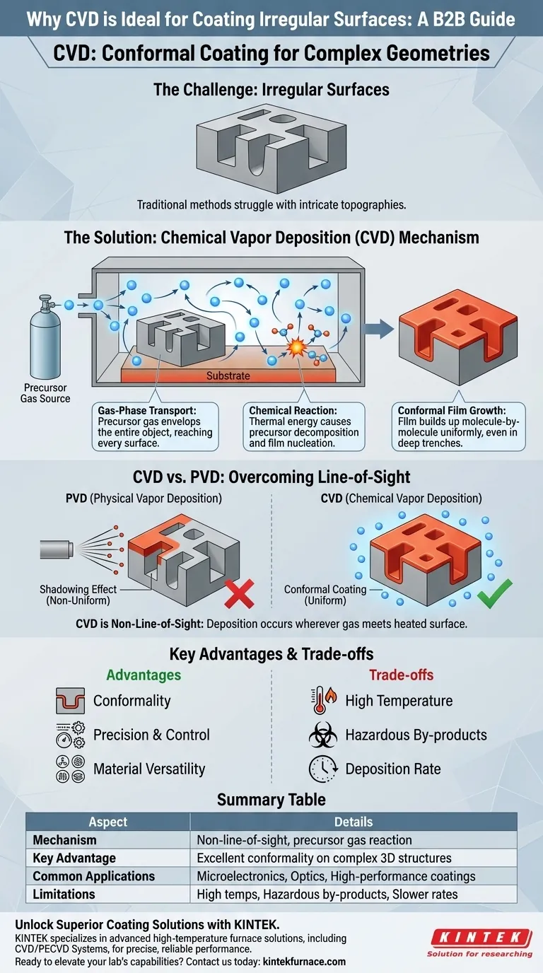
At its core, Chemical Vapor Deposition (CVD) is uniquely suited for coating irregular surfaces because it is not a line-of-sight process. The material to be deposited is introduced as a gas (a precursor) that completely envelops the substrate, allowing a chemical reaction to build a film molecule-by-molecule on every exposed surface simultaneously, regardless of its orientation or complexity.
The fundamental advantage of CVD is its mechanism: a reactive gas fills the entire volume around an object, allowing the coating to "grow" uniformly on all surfaces at once, rather than being "sprayed" from a single direction. This overcomes the shadowing effects that plague other methods.
The Fundamental Mechanism: Gas-Phase Transport
To understand why CVD provides such uniform coverage, you must first understand how the material travels to the surface. The process is fundamentally different from physical deposition methods.
How Precursor Gases Work
In CVD, the coating material doesn't start as a solid that is evaporated or sputtered. Instead, it is introduced into a chamber as a precursor gas.
Like any gas, the precursor molecules move randomly and rapidly, filling the entire volume of the reaction chamber and surrounding the substrate on all sides.
Deposition Through Chemical Reaction
The coating doesn't form until the precursor gas molecules come into contact with the heated substrate. The thermal energy on the substrate's surface triggers a chemical reaction.
This reaction breaks down the precursor molecules, causing the desired solid material to deposit, or "nucleate," directly onto the surface. The film is built up one atomic or molecular layer at a time.
The Result: A Dense, Conformal Film
Because the chemical reaction happens wherever the hot surface and the precursor gas meet, the film grows uniformly across the entire object. This includes the insides of deep trenches, holes, and other complex, non-planar features. The result is a highly dense and pure film with minimal voids.
Why This Excels at Conformality
The term for this ability to coat uniformly over complex topography is conformality. CVD's gas-phase nature gives it a distinct advantage over competing technologies.
Overcoming the "Line-of-Sight" Limitation
Techniques like Physical Vapor Deposition (PVD), such as sputtering or evaporation, are line-of-sight processes. They are analogous to spray painting.
In PVD, atoms are ejected from a solid target and travel in a straight line to the substrate. Surfaces directly facing the source get a thick coating, while vertical sidewalls or the bottoms of trenches receive little to no material, creating a "shadowing" effect.
True Uniformity on 3D Structures
CVD completely avoids this issue. Since the precursor gas surrounds the object, the deposition rate is governed by the chemical reaction on the surface, not the angle of arrival. This allows for nearly perfect, uniform thickness on even the most intricate three-dimensional structures.
Precision and Control
By carefully controlling temperature, pressure, and gas concentrations, CVD allows for precise management of film thickness, composition, and microstructure. This level of control is essential for high-performance applications in fields like microelectronics and optics.
Understanding the Trade-offs
While powerful, CVD is not a universal solution. Understanding its limitations is critical for making an informed decision.
High Temperature Requirements
Traditional thermal CVD processes often require very high temperatures (several hundred to over 1000°C) to initiate the necessary chemical reactions. These temperatures can damage or destroy thermally sensitive substrates, such as plastics or certain integrated circuits.
Complex Chemistry and Hazardous By-products
The chemical reactions that deposit the film also create by-products. These can be toxic, corrosive, or environmentally hazardous, requiring complex and expensive exhaust management systems. The precursor gases themselves are often highly reactive or dangerous.
Deposition Rate and Scalability
While CVD can be scaled for mass production, there is often a trade-off between deposition speed and film quality. Achieving a highly uniform, high-purity film may require slower deposition rates, which can impact throughput and cost.
Making the Right Choice for Your Application
Selecting a deposition technology depends entirely on your project's specific constraints and goals.
- If your primary focus is uniform coating on complex 3D geometries: CVD is almost always the superior choice due to its non-line-of-sight, gas-phase deposition mechanism.
- If your substrate is temperature-sensitive: You must consider low-temperature CVD variants (like Plasma-Enhanced CVD) or explore alternative methods like Atomic Layer Deposition (ALD) or PVD.
- If your priority is depositing a wide variety of materials: CVD is highly versatile and can deposit metals, ceramics, and polymers simply by changing the precursor chemistry.
Ultimately, CVD's power lies in its ability to build high-quality films from the ground up, molecule by molecule, on any surface the precursor gas can reach.
Summary Table:
| Aspect | Details |
|---|---|
| Mechanism | Non-line-of-sight process using precursor gases for uniform coverage |
| Key Advantage | Excellent conformality on complex 3D structures, avoiding shadowing effects |
| Common Applications | Microelectronics, optics, and high-performance coatings |
| Limitations | High temperatures, hazardous by-products, and potential slower deposition rates |
Unlock Superior Coating Solutions with KINTEK
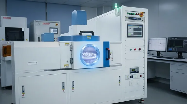
Struggling to achieve dense, uniform films on intricate surfaces? KINTEK specializes in advanced high-temperature furnace solutions tailored to your unique needs. Our CVD/PECVD Systems, part of a comprehensive product line including Muffle, Tube, Rotary, Vacuum & Atmosphere Furnaces, leverage exceptional R&D and in-house manufacturing for precise, reliable performance. With strong deep customization capabilities, we ensure our equipment meets your exact experimental requirements, enhancing efficiency and results in fields like microelectronics and materials science.
Ready to elevate your lab's capabilities? Contact us today to discuss how KINTEK can support your innovative projects!
Visual Guide
Related Products
- Custom Made Versatile CVD Tube Furnace Chemical Vapor Deposition CVD Equipment Machine
- MPCVD Machine System Reactor Bell-jar Resonator for Lab and Diamond Growth
- Multi Heating Zones CVD Tube Furnace Machine for Chemical Vapor Deposition Equipment
- 915MHz MPCVD Diamond Machine Microwave Plasma Chemical Vapor Deposition System Reactor
- Slide PECVD Tube Furnace with Liquid Gasifier PECVD Machine
People Also Ask
- Which industries and research fields benefit from CVD tube furnace sintering systems for 2D materials? Unlock Next-Gen Tech Innovations
- What is a CVD tube furnace and what is its primary function? Discover Precision Thin-Film Deposition
- What future trends are expected in the development of CVD tube furnaces? Discover Smarter, More Versatile Systems
- Why are CVD tube furnace sintering systems indispensable for 2D material research and production? Unlock Atomic-Scale Precision
- How does CVD tube furnace sintering enhance graphene growth? Achieve Superior Crystallinity and High Electron Mobility


