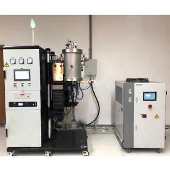
Vacuum thermal evaporation offers superior control over film quality by operating at extremely high vacuum levels, typically around 4 x 10⁻⁶ Torr. This environment allows for the precise deposition of sensitive materials like TPBi, LiF, and aluminum without the interference of atmospheric contaminants.
By eliminating environmental impurities and enabling meticulous thickness regulation, this method ensures the precise energy level alignment and carrier balance necessary for high-performance multi-layer OLED structures.
The Critical Role of the Vacuum Environment
Achieving High-Purity Deposition
The primary technical advantage of this system is the creation of an environment virtually free of contaminants.
Operating at high vacuum levels such as 4 x 10⁻⁶ Torr significantly reduces the presence of background gases.
Eliminating Environmental Impurities
Sensitive organic materials and reactive metals are highly susceptible to degradation.
By removing environmental impurities, the system prevents foreign atoms from embedding into the deposited layers. This is essential for maintaining the chemical integrity of materials like LiF (Lithium Fluoride) and aluminum electrodes.
Precision and Device Physics
Meticulous Thickness Control
Beyond purity, the system allows for the high-precision regulation of film thickness.
This is not merely about physical dimensions; it is about controlling the electronic properties of the device. Even slight deviations in thickness can alter the resistance and optical properties of the layer.
Ensuring Energy Level Alignment
The performance of multi-layer structures, such as OLEDs, relies on how energy bands line up between layers.
Precise deposition ensures that the Electron Transport Layer (using materials like TPBi) aligns correctly with the cathode. This facilitates efficient electron injection and transport.
Optimizing Carrier Balance
For a device to function efficiently, the number of electrons and holes (charge carriers) must be balanced.
The precision of thermal evaporation ensures the deposited layers are uniform and of the exact thickness required to maintain this optimal carrier balance. This directly results in improved device efficiency and stability.
Understanding the Trade-offs
The Necessity of Strict Vacuum Maintenance
While this method yields superior quality, it is heavily dependent on maintaining the vacuum integrity.
If the pressure rises above the 4 x 10⁻⁶ Torr threshold, the mean free path of the evaporant decreases. This can lead to scattering and the reintroduction of impurities, effectively negating the benefits of the process.
Making the Right Choice for Your Goal
To maximize the efficacy of your deposition process, align your operational parameters with your specific structural requirements.
- If your primary focus is Device Efficiency: Prioritize precise thickness monitoring to ensure optimal carrier balance and energy level alignment between the ETL and electrode.
- If your primary focus is Material Longevity: Ensure your vacuum protocols strictly maintain pressures at or below 4 x 10⁻⁶ Torr to prevent environmental contamination of reactive layers.
Precision in the vacuum environment is the single most critical factor in translating raw materials into high-performance electronic structures.
Summary Table:
| Technical Feature | Benefit for Deposition | Impact on Device Performance |
|---|---|---|
| High Vacuum (4x10⁻⁶ Torr) | Eliminates background gases & impurities | Enhances material purity and longevity |
| Precise Thickness Control | Meticulous regulation of film dimensions | Optimizes energy level alignment & resistance |
| Controlled Environment | Prevents degradation of reactive metals (LiF, Al) | Facilitates efficient electron injection |
| Uniform Layering | Consistent material distribution | Ensures optimal carrier balance and stability |
Elevate Your Material Research with KINTEK
Don’t let atmospheric contaminants compromise your high-performance electronic structures. Backed by expert R&D and world-class manufacturing, KINTEK offers a comprehensive range of Muffle, Tube, Rotary, Vacuum, and CVD systems, all precision-engineered to meet your unique thin-film deposition needs.
Whether you are developing next-generation OLEDs or advanced semiconductors, our customizable lab high-temperature furnaces provide the vacuum integrity and meticulous control required for superior device efficiency.
Ready to achieve industry-leading precision? Contact us today to discuss your project and discover the KINTEK advantage.
References
- Dipanshu Sharma, Jwo‐Huei Jou. Two-Dimensional Transition Metal Dichalcogenide: Synthesis, Characterization, and Application in Candlelight OLED. DOI: 10.3390/molecules30010027
This article is also based on technical information from Kintek Furnace Knowledge Base .
Related Products
- Inclined Rotary Plasma Enhanced Chemical Deposition PECVD Tube Furnace Machine
- Custom Made Versatile CVD Tube Furnace Chemical Vapor Deposition CVD Equipment Machine
- Slide PECVD Tube Furnace with Liquid Gasifier PECVD Machine
- RF PECVD System Radio Frequency Plasma Enhanced Chemical Vapor Deposition
- MPCVD Machine System Reactor Bell-jar Resonator for Lab and Diamond Growth
People Also Ask
- How does a CVD system ensure the quality of carbon layers? Achieving Nanometer Precision with KINTEK
- What are the technical advantages of using a CVD system? Optimize Carbon Nanotube Growth for Thermal Conductivity
- What advantages does the Laser Chemical Vapor Deposition (LCVD) process offer? High Purity & Precision SiC Fibers
- What environments does a PECVD system provide for silicon nanowires? Optimize Growth with Precise Thermal Control
- Why Use PECVD for Monolithic Integrated Chip Isolation Layers? Protect Your Thermal Budget with High-Quality SiO2
