In short, PVD (Physical Vapor Deposition) is the superior choice for depositing high-purity films, particularly metals, onto relatively simple geometries where strong adhesion and precise control are critical. While CVD (Chemical Vapor Deposition) is better suited for creating uniform coatings on complex, three-dimensional surfaces, PVD excels when the goal is to transfer a source material to a substrate with minimal chemical alteration.
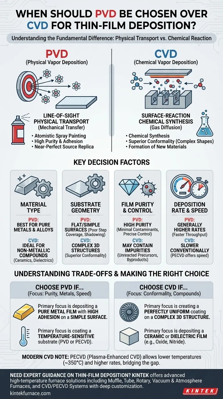
The decision between PVD and CVD hinges on a fundamental distinction: PVD physically transports a material from a source to a substrate, whereas CVD uses a chemical reaction to create a new material directly on the substrate's surface. Understanding this core difference is the key to selecting the right process for your application.
The Fundamental Difference: Physical Transport vs. Chemical Reaction
To make an informed decision, you must first understand the mechanism behind each process. Their names—Physical vs. Chemical—reveal their core nature and dictate their respective strengths and weaknesses.
How PVD Works: The "Line-of-Sight" Method
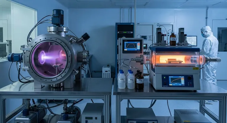
Physical Vapor Deposition is essentially a mechanical transfer process. In methods like sputtering or evaporation, a solid source material (the "target") is bombarded with energy, causing atoms to be ejected.
These atoms travel in a straight line through a vacuum and condense onto the substrate, forming a thin film. Think of it as an atomic-level spray painting process.
This direct, physical transport is why PVD excels at producing films that are exceptionally pure, uniform, and have strong adhesion. The final film is a near-perfect replica of the source material.
How CVD Works: The "Surface-Reaction" Method
Chemical Vapor Deposition is a process of synthesis. It introduces one or more volatile precursor gases into a reaction chamber.
These gases decompose and react on the heated substrate's surface, forming a new, solid material as the desired film. Unwanted byproducts are then exhausted from the chamber.
Because the process is governed by gas diffusion and surface chemistry, CVD can coat intricate and complex geometries with outstanding uniformity, a property known as conformality.
Key Decision Factors for PVD vs. CVD
Your choice will be guided by four primary factors: the material you need to deposit, the shape of your substrate, your required speed, and the level of purity you need.
Material Type: Metals vs. Compounds
PVD is the standard for depositing pure metals and their alloys. The process is ideal for creating targets from these materials and physically transferring them.
CVD is primarily used for depositing non-metallic compounds, such as ceramics (oxides, nitrides, carbides) and other dielectrics. The chemical reaction allows for the synthesis of materials that are difficult or impossible to create as a solid PVD target.
Substrate Geometry: Flat vs. Complex
Due to its line-of-sight nature, PVD is most effective for coating flat or gently curved surfaces. Areas that are not in the direct path of the source material will receive little to no coating, an effect known as "shadowing."
CVD's gas-based process allows it to "flow" into and around complex 3D structures, trenches, and through-holes. If you need a perfectly uniform coating on a non-flat part, CVD offers superior conformality.
Film Purity and Control
PVD offers higher purity films. Since it's a physical transfer in a high vacuum, the risk of incorporating contaminants from precursor gases or chemical byproducts is virtually eliminated. This allows for very precise control over the film's properties.
CVD films can sometimes contain impurities, such as unreacted precursor elements or byproducts from the chemical reaction.
Deposition Rate and Throughput
In general, PVD processes can achieve higher deposition rates than conventional CVD. This makes PVD a more attractive option for applications requiring thicker films or high-throughput manufacturing where speed is a priority.
Understanding the Trade-offs
Neither technology is a silver bullet. Acknowledging their inherent limitations is crucial for avoiding costly mistakes.
The PVD Limitation: Poor Step Coverage
The primary drawback of PVD is its line-of-sight deposition. It cannot effectively coat the sidewalls of deep trenches or the interior of complex parts. This lack of conformality makes it unsuitable for many microfabrication and advanced packaging applications.
The CVD Limitation: Temperature and Impurities
Traditional CVD processes often require very high temperatures to drive the necessary chemical reactions, which can damage temperature-sensitive substrates like polymers or certain electronic components.
Furthermore, the chemical nature of the process means there is always a risk of introducing impurities into the film, which can alter its electrical or mechanical properties.
A Note on Modern CVD Variants
It's important to recognize that CVD technology has evolved. Variants like PECVD (Plasma-Enhanced CVD) use a plasma to energize the precursor gases, allowing deposition to occur at much lower temperatures (e.g., ~350°C). PECVD can also offer high deposition rates, bridging the gap with PVD in certain applications.
Making the Right Choice for Your Goal
Base your decision on your single most important outcome.
- If your primary focus is depositing a pure metal film with high adhesion on a simple surface: PVD is the definitive and most direct solution.
- If your primary focus is creating a perfectly uniform coating on a complex 3D structure: CVD is the only way to achieve the required conformality.
- If your primary focus is depositing a ceramic or dielectric film like an oxide or nitride: CVD is the standard industry process designed for synthesizing these materials.
- If your primary focus is coating a temperature-sensitive substrate: PVD or a low-temperature variant like PECVD are your safest and most effective options.
By aligning the fundamental mechanism of the process with your end goal, you can confidently select the right technology for the job.
Summary Table:
| Factor | PVD (Physical Vapor Deposition) | CVD (Chemical Vapor Deposition) |
|---|---|---|
| Material Type | Best for pure metals and alloys | Ideal for non-metallic compounds (e.g., oxides, nitrides) |
| Substrate Geometry | Suitable for flat or simple surfaces; poor step coverage | Excellent for complex 3D structures; superior conformality |
| Film Purity | High purity with minimal contaminants | May contain impurities from chemical reactions |
| Deposition Rate | Generally higher rates for faster throughput | Slower in conventional forms; PECVD offers faster options |
| Temperature Sensitivity | Lower temperature options available; good for sensitive substrates | High temperatures in traditional CVD; PECVD reduces this issue |
Need expert guidance on selecting the right thin-film deposition solution for your lab? At KINTEK, we leverage exceptional R&D and in-house manufacturing to provide advanced high-temperature furnace solutions tailored to your needs. Our product line includes Muffle, Tube, Rotary Furnaces, Vacuum & Atmosphere Furnaces, and CVD/PECVD Systems, all backed by strong deep customization capabilities to precisely meet your unique experimental requirements. Whether you're working with metals, ceramics, or complex geometries, we can help optimize your process for superior results. Contact us today to discuss how our solutions can enhance your research and development!
Visual Guide
Related Products
- 915MHz MPCVD Diamond Machine Microwave Plasma Chemical Vapor Deposition System Reactor
- HFCVD Machine System Equipment for Drawing Die Nano Diamond Coating
- RF PECVD System Radio Frequency Plasma Enhanced Chemical Vapor Deposition
- Inclined Rotary Plasma Enhanced Chemical Deposition PECVD Tube Furnace Machine
- MPCVD Machine System Reactor Bell-jar Resonator for Lab and Diamond Growth
People Also Ask
- How does the MPCVD process work to deposit diamond? A Guide to High-Purity Synthesis
- What is the MPCVD method and why is it considered effective for diamond deposition? Superior Purity & High Growth Rates
- What are the main components of an MPCVD machine? Unlock the Secrets of Diamond Synthesis
- What are the essential components of an MPCVD reactor for diamond film deposition? Unlock High-Quality Diamond Growth
- In which industries is the microwave plasma chemical vapor deposition system commonly used? Unlock High-Purity Material Synthesis


