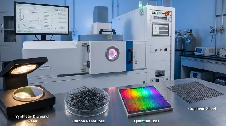
At its core, Chemical Vapor Deposition (CVD) is a remarkably versatile process capable of producing a vast range of high-performance materials. It is used to create everything from simple metallic coatings to advanced nanostructures like synthetic diamond films, graphene, carbon nanotubes, and quantum dots. This precision allows for the engineering of materials with specific properties for industries spanning electronics, aerospace, and medical technology.
The true power of CVD lies not in a specific material it creates, but in its fundamental ability to deposit thin, uniform layers of elements—metals, ceramics, and carbons—and assemble them into highly advanced structures. It is less a single manufacturing method and more a foundational platform for material innovation.
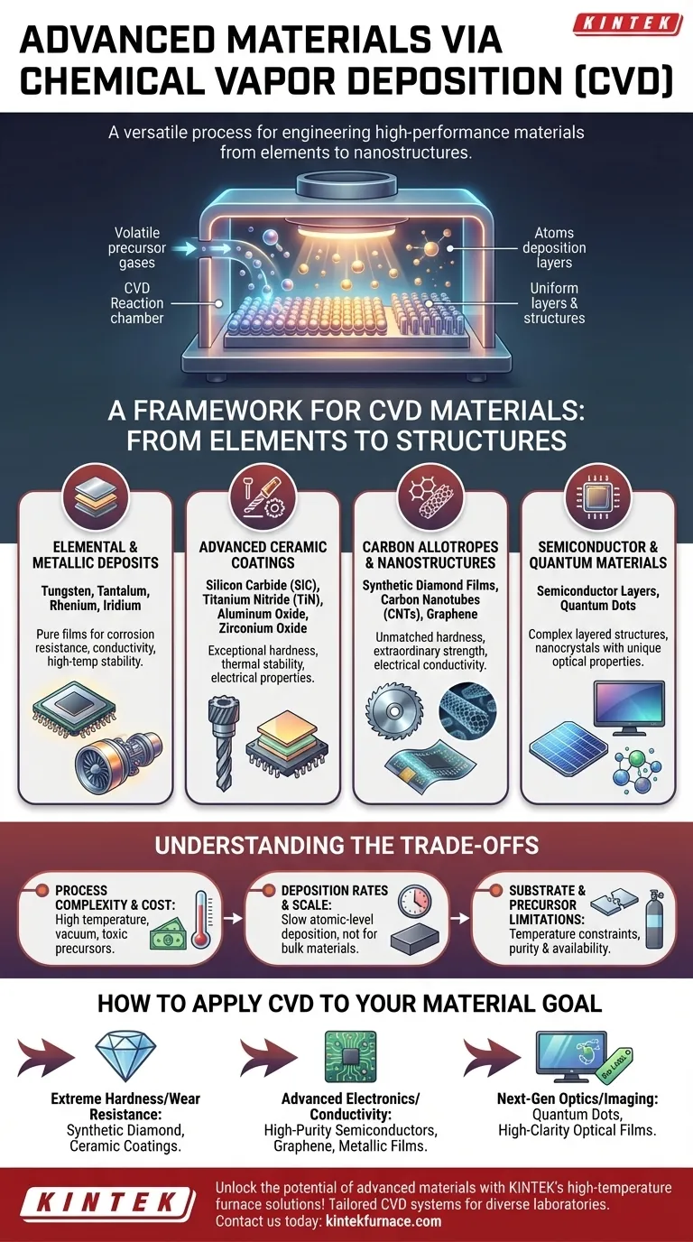
A Framework for CVD Materials: From Elements to Structures
CVD works by introducing a volatile precursor gas into a reaction chamber, which then decomposes and deposits a solid material onto a substrate. The type of precursor gas and process conditions (temperature, pressure) dictate the final material. We can categorize the outputs into several key groups.
Elemental and Metallic Deposits
CVD is highly effective at depositing thin films of extremely pure, high-performance metals. These coatings are often used for their corrosion resistance, conductivity, or high-temperature stability.
Common examples include tungsten, tantalum, rhenium, and iridium. These are crucial in applications like microelectronics and protective coatings in aerospace engines.
Advanced Ceramic Coatings
Ceramics deposited by CVD are prized for their exceptional hardness, thermal stability, and electrical properties. They are broadly divided into two classes.
Non-oxide ceramics include materials like silicon carbide (SiC), tungsten carbide (WC), and titanium nitride (TiN). These are staples for creating durable cutting tools and wear-resistant surfaces.
Oxide ceramics such as aluminum oxide (alumina), zirconium oxide (zirconia), and hafnium oxide (hafnia) are used as thermal barriers and high-performance electrical insulators in semiconductor devices.
Carbon Allotropes and Nanostructures
Some of the most groundbreaking materials produced via CVD are based on carbon. By controlling the atomic arrangement, CVD can produce carbon structures with vastly different properties.
Synthetic diamond films are created for their unmatched hardness, making them ideal for industrial cutting and grinding, as well as for durable optical windows.
Carbon nanotubes (CNTs) and graphene are one-dimensional and two-dimensional carbon structures, respectively. Their extraordinary strength and electrical conductivity make them foundational materials for next-generation electronics, composites, and transparent conductive films.
Semiconductor and Quantum Materials
The electronics industry is fundamentally dependent on CVD. The process is used to build up the complex, layered structures of modern integrated circuits by depositing thin films of semiconductor materials.
Beyond traditional semiconductors, CVD is used to create quantum dots. These are semiconductor nanocrystals whose tiny size gives them unique quantum mechanical and optical properties, essential for advanced displays, solar cells, and biomedical imaging.
Understanding the Trade-offs: Precision vs. Practicality
While CVD is exceptionally powerful, it is not a universally simple solution. The process involves significant trade-offs that must be considered.
Process Complexity and Cost
CVD systems often require high temperatures and vacuum conditions, making the equipment complex and expensive. The precursor gases can also be highly toxic, flammable, or corrosive, requiring stringent safety protocols and handling infrastructure.
Deposition Rates and Scale
CVD is fundamentally a surface deposition process, building material layer by atomic layer. This precision comes at the cost of speed. Deposition rates can be slow, making it less suitable for producing bulk materials or very thick coatings compared to other methods.
Substrate and Precursor Limitations
The choice of substrate material is limited by the high temperatures required for the reaction, which can damage sensitive components. Furthermore, the availability and cost of suitable high-purity precursor gases can constrain the types of materials that can be economically produced.
How to Apply CVD to Your Material Goal
The decision to use CVD should be driven by the specific material property you need to achieve.
- If your primary focus is extreme hardness or wear resistance: CVD is the ideal method for depositing synthetic diamond films or ceramic coatings like titanium nitride and silicon carbide.
- If your primary focus is advanced electronics or conductivity: Look to CVD for creating high-purity semiconductor layers, graphene sheets for flexible electronics, or metallic films for interconnects.
- If your primary focus is next-generation optics or imaging: CVD is the leading technique for producing quantum dots for displays and bio-labels, as well as high-clarity optical films like diamond.
Ultimately, Chemical Vapor Deposition serves as a precise atomic-level tool for engineers and scientists to build the exact material a specific challenge demands.
Summary Table:
| Material Category | Key Examples | Primary Applications |
|---|---|---|
| Elemental and Metallic Deposits | Tungsten, Tantalum | Microelectronics, Protective Coatings |
| Advanced Ceramic Coatings | Silicon Carbide, Titanium Nitride | Cutting Tools, Wear Resistance |
| Carbon Allotropes and Nanostructures | Graphene, Carbon Nanotubes | Next-Gen Electronics, Composites |
| Semiconductor and Quantum Materials | Quantum Dots, Semiconductor Layers | Displays, Solar Cells, Imaging |
Unlock the potential of advanced materials with KINTEK's high-temperature furnace solutions! Leveraging exceptional R&D and in-house manufacturing, we provide diverse laboratories with tailored CVD systems, including Muffle, Tube, Rotary Furnaces, Vacuum & Atmosphere Furnaces, and CVD/PECVD Systems. Our deep customization capability ensures precise alignment with your unique experimental needs, enhancing efficiency and innovation in electronics, aerospace, and medical technology. Contact us today to discuss how our solutions can drive your material goals forward!
Visual Guide
Related Products
- Custom Made Versatile CVD Tube Furnace Chemical Vapor Deposition CVD Equipment Machine
- Split Chamber CVD Tube Furnace with Vacuum Station CVD Machine
- Multi Heating Zones CVD Tube Furnace Machine for Chemical Vapor Deposition Equipment
- Slide PECVD Tube Furnace with Liquid Gasifier PECVD Machine
- Controlled Inert Nitrogen Hydrogen Atmosphere Furnace
People Also Ask
- What is a CVD tube furnace and what is its primary function? Discover Precision Thin-Film Deposition
- What temperature range do standard CVD tube furnaces operate at? Unlock Precision for Your Material Deposition
- What are the key application fields of CVD tube furnaces? Unlock Precision in Thin-Film Synthesis
- What are the benefits of developing new precursor materials for CVD tube furnaces? Unlock Advanced Thin-Film Synthesis
- Why are CVD tube furnace sintering systems indispensable for 2D material research and production? Unlock Atomic-Scale Precision


