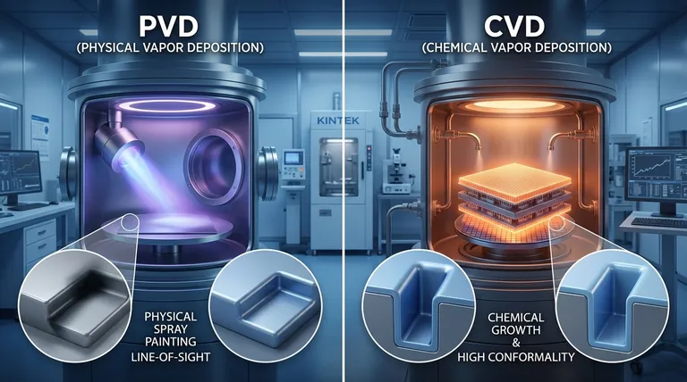
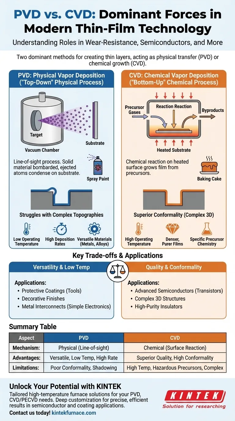
In modern thin-film technology, Physical Vapor Deposition (PVD) and Chemical Vapor Deposition (CVD) are the two dominant methods for creating a thin layer of material on a substrate. PVD acts as a physical "spray painting" process, transferring solid material onto a surface, making it ideal for wear-resistant coatings and metallization. In contrast, CVD is a chemical process that "grows" a film atom-by-atom from gaseous precursors, making it indispensable for creating the highly uniform and complex layers required in advanced semiconductors.
Your choice between PVD and CVD hinges on a fundamental trade-off: PVD offers versatility and lower processing temperatures, while CVD provides superior film quality and the ability to uniformly coat complex three-dimensional structures.
The Core Mechanism: Physical vs. Chemical
Understanding how each process works at an atomic level is the key to selecting the right one for your goal. They represent two fundamentally different philosophies for building a film.
How PVD Works: A "Top-Down" Physical Process
PVD is a line-of-sight process that takes place in a vacuum. A solid source material, known as the "target," is bombarded with energy, causing atoms or molecules to be ejected.
These ejected particles travel in a straight line through the vacuum and condense onto the substrate, forming a thin film. The two most common PVD methods are sputtering (using an ion beam to dislodge atoms) and thermal evaporation (heating the material until it vaporizes).
Think of PVD as an atomic-scale spray paint. The "paint" (source material) is ejected from the can and travels directly to the surface it is aimed at.
How CVD Works: A "Bottom-Up" Chemical Process
CVD is fundamentally a chemical reaction. Volatile precursor gases containing the atoms of the desired film are introduced into a reaction chamber.
The substrate is heated to a specific temperature, which provides the energy needed to trigger a chemical reaction on its surface. The precursor gases react and decompose, depositing a solid film and leaving behind volatile byproducts that are then exhausted.
This process is more like baking a cake. You introduce ingredients (gases) into a hot environment (the reactor), and they chemically transform to create a new solid structure (the film) that covers every surface evenly.
Key Characteristics and Their Impact
The difference in mechanism leads to distinct advantages and disadvantages that dictate their roles in industry.
Film Quality and Conformality
CVD typically produces films that are denser, purer, and more uniform. Because the film is "grown" from a chemical reaction, it can form a highly conformal coating that covers intricate steps, trenches, and complex 3D geometries perfectly.
PVD, being a line-of-sight process, struggles with complex topographies. Protruding features can create "shadows," leading to thin or non-existent coverage in trenches or on sidewalls.
Operating Temperature
PVD is generally a low-temperature process. This makes it suitable for depositing films onto temperature-sensitive substrates, such as plastics or previously fabricated electronic components that cannot withstand high heat.
CVD almost always requires high temperatures (from a few hundred to over a thousand degrees Celsius) to drive the necessary chemical reactions. This limits its use to substrates that are thermally stable, like silicon wafers or ceramics.
Material Versatility and Deposition Rate
PVD is extremely versatile and can be used to deposit a vast range of materials, including pure metals, alloys, and certain ceramic compounds. Deposition rates, especially for metals, can be very high.
CVD processes are highly specific to the desired film material. While it excels at producing ultra-pure films like silicon dioxide, silicon nitride, and tungsten, developing a new CVD process for a novel material can be a significant research and development effort.
Understanding the Trade-offs
Neither method is universally superior; they are tools optimized for different tasks. Objectively weighing their limitations is critical for making an informed decision.
PVD: The Versatile Workhorse
PVD's primary advantage is its flexibility. The ability to operate at low temperatures on a wide variety of materials makes it the go-to choice for protective coatings on tools, decorative finishes on consumer products, and creating the metal interconnects on many integrated circuits.
The main drawback is its poor conformality. For any application requiring a perfectly uniform film over a non-flat surface, PVD is often unsuitable without complex substrate rotation and tilting mechanisms, which still may not solve the problem completely.
CVD: The High-Performance Specialist
CVD's unrivaled conformality and ability to produce high-purity films make it essential for high-performance applications. It is the backbone of modern semiconductor manufacturing, used to create the critical gate oxides and insulating layers in transistors.
Its major limitations are the high processing temperatures, which restrict substrate choices, and the often hazardous and expensive nature of the precursor gases. The process chemistry can also be complex to control.
Making the Right Choice for Your Application
Your final decision must be aligned with the single most important requirement of your film.
- If your primary focus is protective or decorative coatings: PVD's versatility, high deposition rate, and cost-effectiveness make it the superior choice for applications like coating tools, medical implants, or watches.
- If your primary focus is advanced semiconductor fabrication: CVD is non-negotiable for creating the highly conformal, defect-free dielectric and barrier layers inside modern microchips.
- If your primary focus is coating temperature-sensitive materials: PVD is the clear winner due to its fundamentally lower operating temperature, enabling coatings on polymers and other delicate substrates.
- If your primary focus is creating simple metal layers for electronics: PVD is often faster and more straightforward for depositing conductive films like aluminum or copper interconnects.
By understanding the core distinction between PVD's physical transfer and CVD's chemical creation, you can confidently select the technology that best serves your engineering goals.
Summary Table:
| Aspect | PVD (Physical Vapor Deposition) | CVD (Chemical Vapor Deposition) |
|---|---|---|
| Mechanism | Physical process; line-of-sight deposition | Chemical process; surface reaction and growth |
| Key Advantages | Versatile, low-temperature operation, high deposition rates | Superior film quality, high conformality, uniform coverage |
| Common Applications | Wear-resistant coatings, metallization, decorative finishes | Advanced semiconductors, complex 3D structures, high-purity films |
| Limitations | Poor conformality, struggles with complex topographies | High temperatures required, complex chemistry, hazardous precursors |
Unlock the Full Potential of Your Thin-Film Applications with KINTEK
Struggling to choose between PVD and CVD for your specific needs? At KINTEK, we leverage exceptional R&D and in-house manufacturing to provide advanced high-temperature furnace solutions tailored to your unique requirements. Our product line includes Muffle, Tube, Rotary Furnaces, Vacuum & Atmosphere Furnaces, and CVD/PECVD Systems, all backed by strong deep customization capabilities. Whether you're working on semiconductor fabrication, protective coatings, or temperature-sensitive materials, we can help you achieve precise, efficient results. Don't let process limitations hold you back—contact us today to discuss how our solutions can enhance your laboratory's performance and drive innovation!
Visual Guide
Related Products
- HFCVD Machine System Equipment for Drawing Die Nano Diamond Coating
- RF PECVD System Radio Frequency Plasma Enhanced Chemical Vapor Deposition
- 915MHz MPCVD Diamond Machine Microwave Plasma Chemical Vapor Deposition System Reactor
- Custom Made Versatile CVD Tube Furnace Chemical Vapor Deposition CVD Equipment Machine
- Cylindrical Resonator MPCVD Machine System for Lab Diamond Growth
People Also Ask
- What is the function of high-purity Argon (Ar) gas during CVD? Optimize Your Thin Film Uniformity and Purity
- What role does Chemical Vapor Deposition (CVD) equipment play in the surface coating of carbon fibers for composites?
- How can customers maximize the quality of CVD coatings? Master Pre-Coating Prep for Superior Results
- What are the equipment for chemical vapor deposition? A Guide to the 5 Essential Components
- What is the significance of the vacuum pressure control system in the CVD coating process for powders?


