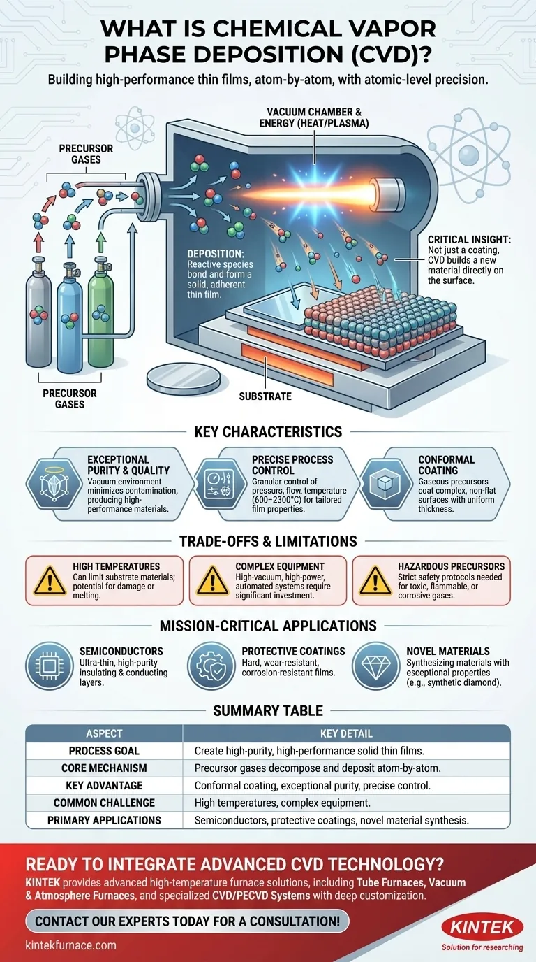
In essence, Chemical Vapor Deposition (CVD) is a highly controlled manufacturing process used to create exceptionally pure, high-performance solid thin films. It works by introducing reactive gases, known as precursors, into a vacuum chamber where they react and decompose, depositing a solid layer atom-by-atom onto a target object or substrate.
The critical insight is not just that CVD creates a coating, but that it builds a new material layer directly on a surface with atomic-level precision. This method is fundamental to producing the high-purity, high-performance materials required for advanced electronics and other demanding applications.
The Core Mechanism: From Gas to Solid Film
To understand CVD, it's best to break it down into its fundamental steps. The entire process takes place within a sealed, low-pressure chamber to ensure absolute purity.
Introducing the Precursors
The process begins by feeding specific volatile gases, or precursors, into the vacuum chamber. These gases contain the chemical elements that will make up the final solid film.
The Role of Energy and Vacuum
The chamber is kept under a high vacuum, which removes unwanted atmospheric contaminants that could compromise the film's quality. Energy, typically in the form of high heat or a plasma discharge, is then applied. This energy breaks down the precursor gases into highly reactive chemical species.
Deposition on the Substrate
These reactive species then travel to the cooler surface of the target object, known as the substrate. They settle on this surface and bond with it, forming a stable, non-volatile solid film. This deposition happens molecule by molecule, creating a dense, uniform, and highly adherent layer.
Key Characteristics of the CVD Process
CVD is valued for a unique combination of characteristics that make it indispensable in high-tech manufacturing.
Exceptional Purity and Quality
Because the process occurs in a vacuum, leakage from the atmosphere is minimized. This, combined with a well-designed reactor, prevents contamination and results in the production of high-quality, high-performance solid materials.
Precise Process Control
Modern CVD systems offer granular control over key variables. Parameters like the working pressure, gas flow rates, and temperature (which can range from 600–2300°C) can be precisely managed. This allows engineers to fine-tune the growth rate, thickness, and final properties of the film.
Conformal Coating Capability
Since the precursors are in a gaseous state, they can penetrate and coat complex, non-flat surfaces with a uniform thickness. This ability to create a conformal coating is a significant advantage over line-of-sight deposition methods like sputtering.
Understanding the Trade-offs and Limitations
While powerful, CVD is not a universal solution. Understanding its inherent challenges is key to its proper application.
High Temperature Requirements
Many CVD processes require very high temperatures to break down the precursor gases. This can limit the types of substrate materials that can be used, as some may be unable to withstand the heat without being damaged or melting.
Complex and Expensive Equipment
CVD systems are sophisticated pieces of machinery. They require high-vacuum pumps, precise gas handling systems, high-power energy sources, and often, fully automated controls. This complexity results in a high initial investment and significant maintenance overhead.
Use of Hazardous Precursors
The gases used as precursors are often toxic, flammable, or corrosive. This necessitates strict safety protocols, specialized handling equipment, and exhaust gas treatment systems, adding to the operational complexity and cost.
Where CVD is Mission-Critical
The choice to use CVD is driven by the need for performance that other methods cannot achieve. Its application depends entirely on the end goal.
- If your primary focus is manufacturing advanced semiconductors: CVD is non-negotiable for depositing the ultra-thin, high-purity insulating and conducting layers that form the foundation of microchips.
- If your primary focus is creating durable protective coatings: CVD is used to apply hard, wear-resistant, and corrosion-resistant films on everything from automotive sensors to consumer electronics.
- If your primary focus is developing novel materials: CVD is a key research tool used to synthesize materials with exceptional properties, such as creating synthetic diamond films for industrial or optical use.
Chemical Vapor Deposition is a cornerstone technology for building the high-performance materials that drive modern innovation.
Summary Table:
| Aspect | Key Detail |
|---|---|
| Process Goal | Create high-purity, high-performance solid thin films. |
| Core Mechanism | Reactive gases (precursors) decompose in a vacuum chamber and deposit a solid layer atom-by-atom onto a substrate. |
| Key Advantage | Conformal coating of complex shapes with exceptional purity and precise control. |
| Common Challenge | Often requires high temperatures and complex, expensive equipment. |
| Primary Applications | Semiconductor manufacturing, durable protective coatings, novel material synthesis (e.g., synthetic diamond). |
Ready to Integrate Advanced CVD Technology into Your Research?
Leveraging exceptional R&D and in-house manufacturing, KINTEK provides diverse laboratories with advanced high-temperature furnace solutions. Our product line, including Tube Furnaces, Vacuum & Atmosphere Furnaces, and specialized CVD/PECVD Systems, is complemented by our strong deep customization capability to precisely meet your unique experimental requirements for thin-film deposition.
Let's discuss how our solutions can enhance your material synthesis and coating processes. Contact our experts today for a tailored consultation!
Visual Guide
Related Products
- Custom Made Versatile CVD Tube Furnace Chemical Vapor Deposition CVD Equipment Machine
- RF PECVD System Radio Frequency Plasma Enhanced Chemical Vapor Deposition
- MPCVD Machine System Reactor Bell-jar Resonator for Lab and Diamond Growth
- Slide PECVD Tube Furnace with Liquid Gasifier PECVD Machine
- 915MHz MPCVD Diamond Machine Microwave Plasma Chemical Vapor Deposition System Reactor
People Also Ask
- Which industries and research fields benefit from CVD tube furnace sintering systems for 2D materials? Unlock Next-Gen Tech Innovations
- What temperature range do standard CVD tube furnaces operate at? Unlock Precision for Your Material Deposition
- How might AI and machine learning enhance CVD tube furnace processes? Boost Quality, Speed, and Safety
- What is a CVD tube furnace and what is its primary function? Discover Precision Thin-Film Deposition
- Why are CVD tube furnace sintering systems indispensable for 2D material research and production? Unlock Atomic-Scale Precision


