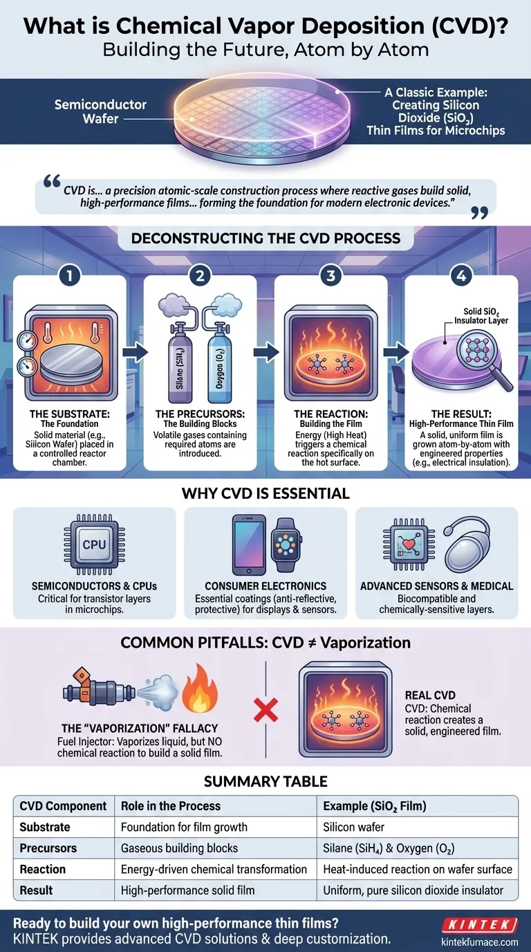
A classic example of chemical vapor deposition (CVD) is the process used in semiconductor manufacturing to deposit a thin film of silicon dioxide (SiO₂) onto a silicon wafer. In this process, precursor gases—such as silane (SiH₄) and oxygen (O₂)—are introduced into a vacuum chamber containing the heated wafer. The high temperature causes the gases to react and decompose on the wafer's surface, forming a solid, uniform, and highly pure layer of glass-like silicon dioxide, one layer of atoms at a time.
Chemical vapor deposition is not simply about turning a liquid into a gas. It is a precision atomic-scale construction process where reactive gases are used to build solid, high-performance films on a surface, forming the foundation for virtually all modern electronic devices.
Deconstructing the CVD Process
To understand what makes CVD so powerful, it is best to break it down into its core components, using the creation of a microchip as our guide.
The Substrate: The Foundation
The process begins with a substrate, which is the material upon which the film will be grown. In semiconductor manufacturing, this is typically a highly pure silicon wafer.
The substrate is placed inside a reactor chamber where conditions like temperature and pressure can be precisely controlled.
The Precursors: The Building Blocks
Next, one or more volatile precursors are introduced into the chamber as gases. These are chemical compounds that contain the atoms needed for the final film.
For a silicon dioxide film, the precursors are the source of silicon (from silane gas) and oxygen (from oxygen gas).
The Reaction: Building the Film
This is the heart of the CVD process. Energy, usually in the form of high heat, is applied to the chamber. This energy causes the precursor gases to undergo a chemical reaction specifically on the hot surface of the substrate.
The precursors decompose and their atoms arrange themselves into a new, solid material, forming a stable and uniform thin film. This layer is grown atom-by-atom, ensuring exceptional purity and control.
The Result: A High-Performance Thin Film
The final result is a solid film bonded to the substrate with specific, engineered properties. The silicon dioxide layer created in our example is an excellent electrical insulator.
This insulating layer is what allows billions of microscopic transistors to be packed onto a single chip without short-circuiting, enabling the power and complexity of modern processors.
Why CVD is Essential in Modern Technology
CVD is not an obscure industrial process; it is a foundational technology that enables the devices we use every day. The films it creates are critical for performance and functionality across many industries.
In Semiconductors and CPUs
CVD is used to create the critical insulating, conductive, and semiconducting layers that form transistors, the building blocks of all microchips. Without CVD, manufacturing modern CPUs would be impossible.
In Consumer Electronics
From smartphones and wearables to smart home devices, CVD is used to apply essential coatings. These can include anti-reflective coatings for displays, protective layers for sensors, and moisture barriers for sensitive electronics.
In Advanced Sensors and Medical Devices
CVD can deposit biocompatible films on medical implants or create chemically-sensitive layers for environmental and biosensors. This allows sensors to interact with their environment or the human body safely and effectively.
Common Pitfalls and Misconceptions
To truly understand CVD, it is critical to separate it from simpler processes that may seem similar on the surface.
The "Vaporization" Fallacy
An automotive fuel injector, which vaporizes liquid fuel for combustion, is not an example of CVD. While it involves vaporization, it completely lacks the most critical step: a chemical reaction that deposits a solid, engineered film onto a surface.
CVD is a deposition process, not a combustion or vaporization process. The goal is to build a solid material, not to burn a fuel.
High-Performance Comes at a Cost
CVD is a complex and demanding process. It requires a vacuum environment, high temperatures, and extremely precise control over gas flows and pressure.
This complexity makes it more expensive than simple coating methods like painting or dipping, which is why it is reserved for applications where performance and purity are paramount.
Making the Right Choice for Your Goal
Understanding CVD allows you to recognize its role in creating high-performance materials and products.
- If your primary focus is electronics manufacturing: CVD is the non-negotiable standard for building the layered architecture of microchips and integrated circuits.
- If your primary focus is materials science: CVD is an indispensable tool for synthesizing novel thin films with specific optical, electrical, or mechanical properties.
- If your primary focus is product design: You can leverage components or apply final CVD coatings to enhance product durability, functionality, and resistance to environmental factors.
Ultimately, chemical vapor deposition is the invisible craft of building materials from the atom up, making it a true cornerstone of our technological world.
Summary Table:
| CVD Component | Role in the Process | Example (SiO₂ Film) |
|---|---|---|
| Substrate | Foundation for film growth | Silicon wafer |
| Precursors | Gaseous building blocks | Silane (SiH₄) & Oxygen (O₂) |
| Reaction | Energy-driven chemical transformation | Heat-induced reaction on wafer surface |
| Result | High-performance solid film | Uniform, pure silicon dioxide insulator |
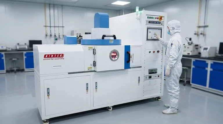
Ready to build your own high-performance thin films? At KINTEK, we leverage our exceptional R&D and in-house manufacturing to provide advanced CVD solutions for diverse laboratories. Our product line, including CVD/PECVD Systems, is complemented by strong deep customization capabilities to precisely meet your unique experimental requirements. Contact us today to discuss how our CVD technology can enhance your research or production process!
Visual Guide
Related Products
- Custom Made Versatile CVD Tube Furnace Chemical Vapor Deposition CVD Equipment Machine
- RF PECVD System Radio Frequency Plasma Enhanced Chemical Vapor Deposition
- MPCVD Machine System Reactor Bell-jar Resonator for Lab and Diamond Growth
- 915MHz MPCVD Diamond Machine Microwave Plasma Chemical Vapor Deposition System Reactor
- Slide PECVD Tube Furnace with Liquid Gasifier PECVD Machine
People Also Ask
- What is the working principle of a CVD tube furnace? Achieve Precise Thin Film Deposition for Your Lab
- What improvements can be made to the bonding force of gate dielectric films using a CVD tube furnace? Enhance Adhesion for Reliable Devices
- How might AI and machine learning enhance CVD tube furnace processes? Boost Quality, Speed, and Safety
- What are the benefits of developing new precursor materials for CVD tube furnaces? Unlock Advanced Thin-Film Synthesis
- What is a CVD tube furnace and what is its primary function? Discover Precision Thin-Film Deposition


