The primary technical advantage of using an Atomic Layer Deposition (ALD) system over Physical Vapor Deposition (PVD) lies in its ability to achieve precise, atomic-level control through self-limiting gas-solid chemical reactions. Unlike PVD, which can struggle with complex geometries, ALD produces Ge-doped Zinc Oxide (Ge:ZnO) films that are highly uniform, pinhole-free, and offer superior step coverage—qualities essential for modern nanoscale device integration.
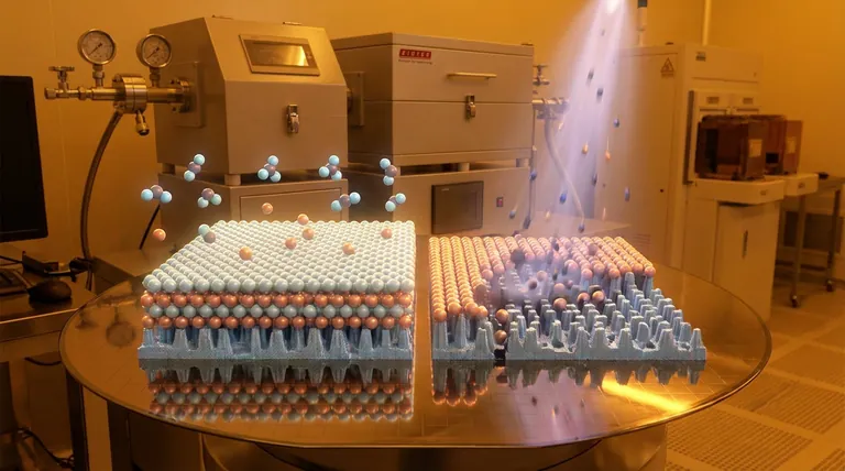
Core Takeaway While traditional PVD methods often rely on directional deposition that can lead to shadowing and uneven coatings, ALD utilizes a self-limiting chemical process. This ensures that every surface of a complex nanostructure receives a perfectly uniform, conformal coating of Ge:ZnO, regardless of the substrate's topography or size.
Achieving Atomic-Level Precision
The Self-Limiting Mechanism
The defining characteristic of ALD is its use of self-limiting gas-solid chemical reactions.
In this process, precursor gases react with the surface one atomic layer at a time. This allows you to dictate the film's thickness and the Ge-doping composition with absolute exactitude, ensuring the Ge:ZnO ratio meets specific performance requirements.
Compositional Control
For doped materials like Ge:ZnO, consistency is paramount for electrical and optical performance.
ALD systems allow you to cycle specific precursors to introduce Germanium dopants into the Zinc Oxide lattice at precise intervals. This eliminates the gradients or segregation often found in bulk PVD deposition methods.
Solving the Geometry Challenge
Superior Step Coverage
A major limitation of traditional PVD is its "line-of-sight" nature, which often results in poor coverage on vertical walls or deep trenches.
ALD overcomes this by chemically saturating the surface. This results in superior step coverage, ensuring the film thickness is identical on all surfaces of a 3D structure, a critical requirement for integrating nanoscale semiconductor devices.
Eliminating Defects
PVD processes can sometimes introduce voids or pinholes, particularly when coating large or irregular areas.
Because ALD builds the film layer by layer, it inherently creates pinhole-free films. This structural integrity is vital for preventing electrical shorts and ensuring the reliability of large-area substrates.
Understanding the Trade-offs
Process Throughput
It is important to acknowledge that the precision of ALD comes at the cost of deposition speed.
Because the film is built one atomic layer at a time, the accumulation rate is significantly lower than that of PVD. ALD is a process optimized for quality and conformity, not raw throughput speed.
Complexity of Operation
Achieving the perfect Ge:ZnO stoichiometry requires precise management of precursor pulses and purge cycles.
While the outcome is superior, the process recipe development in ALD can be more complex than setting parameters for a standard sputtering or evaporation target in PVD.
Making the Right Choice for Your Goal
To determine if ALD is the correct tool for your Ge:ZnO fabrication, evaluate your specific constraints:
- If your primary focus is Nanoscale Integration: Choose ALD for its ability to coat complex, 3D geometries with perfect conformity and step coverage.
- If your primary focus is Film Integrity: Choose ALD to ensure a pinhole-free structure critical for high-reliability semiconductor applications.
- If your primary focus is Precise Doping: Choose ALD for its capability to control the Germanium-to-Zinc ratio at the atomic level.
For advanced semiconductor applications where geometry is complex and tolerance for defects is zero, ALD is not just an alternative to PVD—it is a necessity.
Summary Table:
| Feature | Atomic Layer Deposition (ALD) | Physical Vapor Deposition (PVD) |
|---|---|---|
| Mechanism | Self-limiting surface reactions | Line-of-sight physical process |
| Thickness Control | Atomic-level precision | Less precise, bulk deposition |
| Conformality | 100% (High aspect ratio structures) | Poor (Shadowing effects) |
| Doping Uniformity | Excellent (Cycle-by-cycle control) | Variable (Gradients possible) |
| Film Quality | Pinhole-free and dense | Potential for voids/defects |
| Deposition Speed | Slower (Layer-by-layer) | Faster (Bulk accumulation) |
Elevate Your Thin Film Precision with KINTEK
Ready to transition from traditional PVD to high-performance ALD for your Ge:ZnO applications? KINTEK provides industry-leading semiconductor solutions backed by expert R&D and manufacturing. We offer a comprehensive range of deposition systems, including ALD, CVD, and Vacuum systems, all of which are fully customizable to meet your specific research or production needs.
Ensure perfect stoichiometry and superior step coverage for your next project. Contact our technical team today to find the ideal system for your lab!
References
- Rafał Knura, Robert P. Socha. Evaluation of the Electronic Properties of Atomic Layer Deposition-Grown Ge-Doped Zinc Oxide Thin Films at Elevated Temperatures. DOI: 10.3390/electronics13030554
This article is also based on technical information from Kintek Furnace Knowledge Base .
Related Products
- HFCVD Machine System Equipment for Drawing Die Nano Diamond Coating
- RF PECVD System Radio Frequency Plasma Enhanced Chemical Vapor Deposition
- 915MHz MPCVD Diamond Machine Microwave Plasma Chemical Vapor Deposition System Reactor
- Cylindrical Resonator MPCVD Machine System for Lab Diamond Growth
- Inclined Rotary Plasma Enhanced Chemical Deposition PECVD Tube Furnace Machine
People Also Ask
- What is chemical vapor deposition (CVD) and its primary industrial application? Unlock Precision Thin Films for Electronics
- What are the equipment for chemical vapor deposition? A Guide to the 5 Essential Components
- What role does Chemical Vapor Deposition (CVD) equipment play in the surface coating of carbon fibers for composites?
- What is the advantage of using a CVD system for coating turbine blades? Master Complex Geometries with Ease
- What is the function of high-purity Argon (Ar) gas during CVD? Optimize Your Thin Film Uniformity and Purity


