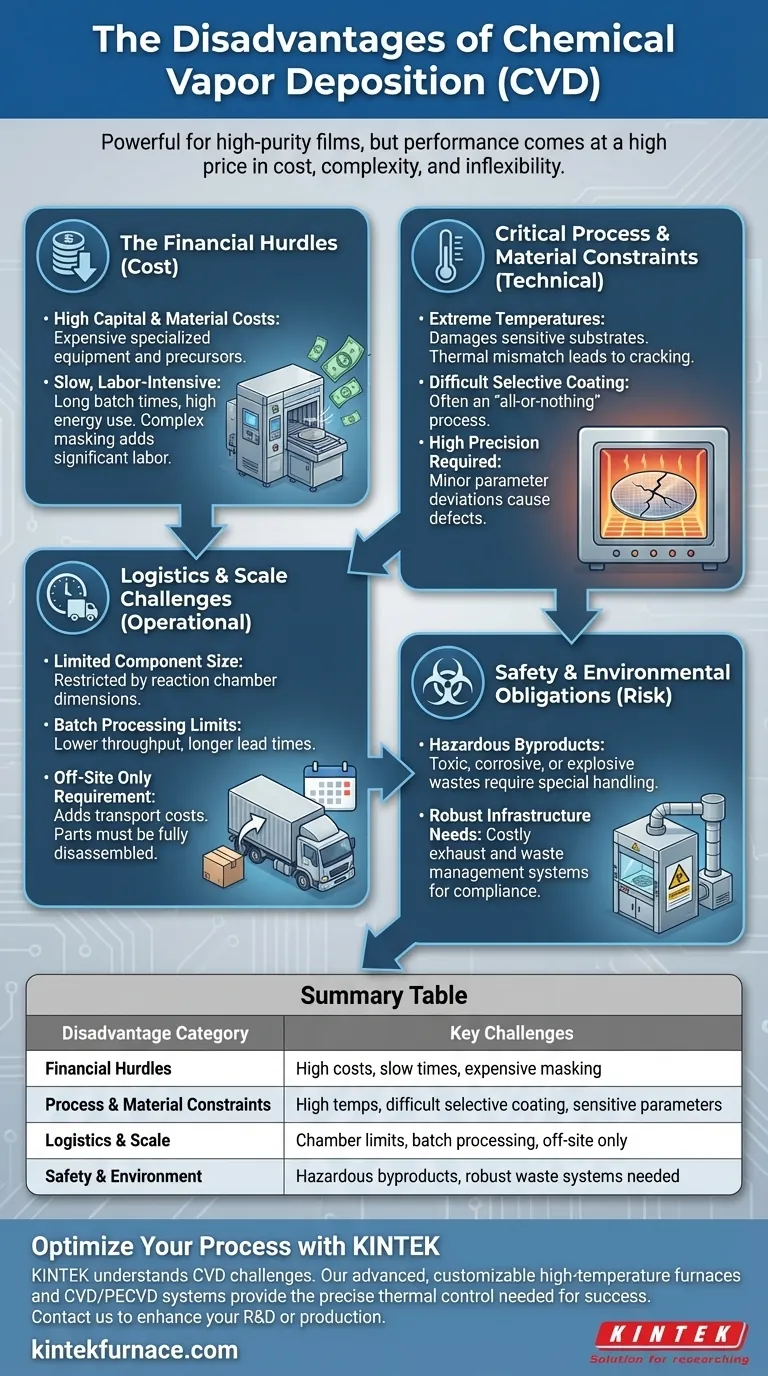
While Chemical Vapor Deposition (CVD) is a powerful technology known for creating high-purity, uniform films, it is not a universally applicable solution. Its primary disadvantages stem from high operational costs, restrictive process requirements like extreme heat, significant logistical complexities, and inherent safety challenges associated with the materials used.
The core issue with CVD is that its exceptional performance comes at a high price in terms of cost, complexity, and inflexibility. Understanding these drawbacks is critical to determining if its benefits truly outweigh the demanding operational requirements for your specific application.
The Financial Hurdles of CVD
The decision to use CVD is often constrained by its significant financial investment, which extends beyond the initial equipment purchase.
High Equipment and Precursor Costs
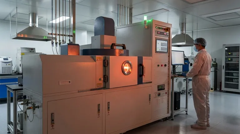
The upfront cost for a CVD reactor and its associated control systems is substantial. This is a highly specialized piece of equipment that demands precise control over the deposition environment.
Furthermore, the raw materials, known as precursors, can be very expensive. This is especially true for metal-organic compounds or specialized gases required to deposit certain high-performance films.
The Hidden Costs of Process Time
CVD is not a rapid process. Deposition can take many hours (sometimes 10-20) to achieve the desired film thickness and quality, leading to high operational and energy costs per batch.
Additionally, selectively coating a part is difficult. The process often requires extensive masking to protect areas that should not be coated. This masking and subsequent demasking is a labor-intensive step that can represent a major portion of the total cost.
Critical Process and Material Constraints
Beyond the cost, the physics of the CVD process itself imposes several key limitations that can exclude it as a viable option.
The High-Temperature Problem
Many CVD processes require very high temperatures to initiate the necessary chemical reactions. This heat can damage or destroy substrates that are not thermally stable, such as polymers or certain metal alloys.
Even if a substrate can withstand the heat, a mismatch in the thermal expansion coefficients between the substrate and the deposited film can create immense internal stress, leading to cracking or delamination of the coating upon cooling.
The Challenge of Selective Coating
As mentioned, masking parts for CVD is difficult and expensive. For many applications, this results in an "all-or-nothing" coating, where the entire component is coated. This is unsuitable if only a specific functional surface requires the film.
The Need for Process Precision
The quality of a CVD film is acutely sensitive to process parameters. Minor deviations in temperature, pressure, or gas flow rates can lead to significant defects in the final coating, compromising its integrity and performance.
Understanding the Trade-offs: Logistics and Scale
The practical implementation of CVD introduces logistical hurdles that differ significantly from more portable coating methods.
Chamber Size and Batch Processing Limits
The size of the components that can be coated is strictly limited by the dimensions of the reaction chamber. This restricts the application of CVD for very large parts.
Because it is a batch process, throughput is limited, which can increase lead times, especially for high-volume production.
The "Off-Site Only" Requirement
CVD is not a process that can be performed on-site. Parts must be shipped to a specialized coating center, which adds transportation costs and logistical complexity to the production workflow.
This also means that assemblies must be completely broken down into individual components before being sent for coating, a time-consuming and labor-intensive requirement.
Safety and Environmental Obligations
The chemical nature of CVD necessitates a strict and costly approach to safety and waste management.
Handling Hazardous Byproducts
The chemical reactions in CVD often produce hazardous byproducts. These can be toxic, corrosive, or even explosive, requiring sophisticated handling and mitigation procedures to ensure personnel safety.
The Need for Robust Infrastructure
Due to these dangerous byproducts, facilities must invest in robust exhaust and waste management systems. This infrastructure is essential for neutralizing harmful substances and complying with environmental regulations, adding another layer of operational cost and complexity.
Making the Right Choice for Your Application
Ultimately, selecting CVD depends on a clear-eyed assessment of its demanding requirements against the performance needs of your component.
- If your primary focus is ultimate performance: The high cost and complexity of CVD are justified when you require a perfectly conformal, pinhole-free coating on a complex geometry that no other method can achieve.
- If your primary focus is cost-sensitive or high-volume production: The high operational costs, batch processing, and logistical overhead of CVD may make alternative methods like PVD (Physical Vapor Deposition) or electroplating more economical.
- If your primary focus is coating heat-sensitive materials: The high-temperature nature of most CVD processes is a definitive barrier, and you should immediately investigate low-temperature deposition alternatives.
Choosing the right coating technology is about aligning the process capabilities with your project's specific goals and constraints.
Summary Table:
| Disadvantage Category | Key Challenges |
|---|---|
| Financial Hurdles | High equipment & precursor costs, slow deposition times, expensive masking requirements |
| Process & Material Constraints | High temperatures damage substrates, difficult selective coating, sensitive process parameters |
| Logistics & Scale | Limited by chamber size, batch processing, off-site coating requirement |
| Safety & Environment | Hazardous byproducts, need for robust exhaust and waste management systems |
Need a high-performance furnace solution without the drawbacks of standard CVD?
At KINTEK, we understand that achieving perfect thin films requires precise thermal control. While CVD has its challenges, our advanced high-temperature furnaces are engineered to provide the stability and uniformity critical for successful deposition processes.
Leveraging exceptional R&D and in-house manufacturing, KINTEK provides diverse laboratories with advanced high-temperature furnace solutions. Our product line, including Muffle, Tube, Rotary Furnaces, Vacuum & Atmosphere Furnaces, and CVD/PECVD Systems, is complemented by our strong deep customization capability to precisely meet unique experimental requirements.
Let us help you optimize your process. Contact our experts today to discuss how our furnace technology can enhance your R&D or production.
Visual Guide
Related Products
- Custom Made Versatile CVD Tube Furnace Chemical Vapor Deposition CVD Equipment Machine
- RF PECVD System Radio Frequency Plasma Enhanced Chemical Vapor Deposition
- MPCVD Machine System Reactor Bell-jar Resonator for Lab and Diamond Growth
- 915MHz MPCVD Diamond Machine Microwave Plasma Chemical Vapor Deposition System Reactor
- Slide PECVD Tube Furnace with Liquid Gasifier PECVD Machine
People Also Ask
- What future trends are expected in the development of CVD tube furnaces? Discover Smarter, More Versatile Systems
- What are the practical applications of gate media prepared by CVD tube furnaces? Unlock Advanced Electronics and More
- Which industries and research fields benefit from CVD tube furnace sintering systems for 2D materials? Unlock Next-Gen Tech Innovations
- What are the key application fields of CVD tube furnaces? Unlock Precision in Thin-Film Synthesis
- What is a CVD tube furnace and what is its primary function? Discover Precision Thin-Film Deposition


