In modern microfabrication, Plasma-Enhanced Chemical Vapor Deposition (PECVD) of silicon dioxide (SiO₂) is a foundational process used to create high-quality thin films. These films serve critical functions, primarily acting as electrical insulators in semiconductors, protective passivation layers against environmental damage, and transparent coatings for optical and photonic devices.
The core value of using PECVD to deposit silicon dioxide is its ability to produce uniform, dense, and conformal insulating films at low temperatures. This low-temperature capability is essential for fabricating complex, multi-layered devices where high heat would damage previously fabricated components.
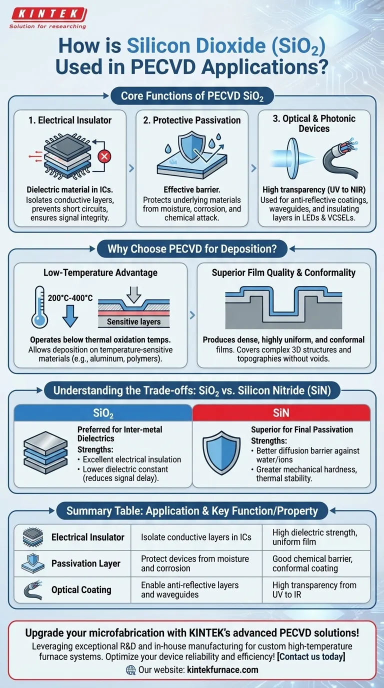
The Core Functions of PECVD SiO₂
Silicon dioxide deposited via PECVD is valued for its specific combination of electrical, chemical, and optical properties. These properties make it a versatile tool for device engineers and researchers.
As a High-Quality Electrical Insulator
The most common application of PECVD SiO₂ is as a dielectric material in integrated circuits. It is used to electrically isolate conductive layers, such as the metal interconnects that wire a chip together.
This isolation prevents short circuits and ensures that signals travel along their intended paths. The quality and uniformity of the PECVD film are critical for device reliability and performance.
As a Protective Passivation Layer
PECVD SiO₂ films form an effective barrier that passivates the surface of a device. This protects sensitive underlying materials from moisture, chemical attack, and other forms of corrosion.
While not as robust a moisture barrier as silicon nitride, it provides essential protection during intermediate fabrication steps and in less demanding environments.
For Optical and Photonic Devices
Due to its excellent transparency across a wide spectrum of light (from UV to near-infrared), SiO₂ is a key material in optics and photonics.
It is used to create anti-reflective coatings, optical waveguides, and insulating layers in devices like high-brightness LEDs and vertical-cavity surface-emitting lasers (VCSELs).
Why Choose PECVD for Deposition?
The choice of deposition method is as important as the choice of material. PECVD offers distinct advantages over other methods, such as thermal oxidation, especially for complex device structures.
The Low-Temperature Advantage
The defining benefit of PECVD is its low operating temperature, typically between 200°C and 400°C. This is significantly lower than the temperatures required for thermal oxidation or other CVD processes.
This allows SiO₂ to be deposited on top of temperature-sensitive materials, such as aluminum interconnects or polymer layers, without causing damage or diffusion.
Superior Film Quality and Conformality
PECVD produces films that are dense, highly uniform across the wafer, and conformal. Conformality means the film coats evenly over the steps and trenches of a device's surface topography.
This ability to cover complex 3D structures without creating voids or weak points is crucial for building reliable, high-density semiconductor devices and MEMS.
Understanding the Trade-offs: SiO₂ vs. Silicon Nitride
In many applications, the choice is not just whether to use PECVD, but which dielectric material to deposit. The most common alternative to SiO₂ is silicon nitride (SiN).
When to Use Silicon Dioxide (SiO₂)
SiO₂ is the preferred choice for inter-metal dielectrics—the insulating layers between wiring levels within a chip. Its primary strengths are its excellent electrical insulation and lower dielectric constant compared to SiN, which helps reduce signal delay.
When to Use Silicon Nitride (SiN)
PECVD SiN is superior as a final passivation layer for encapsulation. It is a significantly better diffusion barrier against water and mobile ions like sodium, offering robust protection from the environment.
Furthermore, SiN possesses greater mechanical hardness and thermal stability, making it ideal for creating durable protective coatings on biomedical devices and MEMS.
Making the Right Choice for Your Goal
Selecting the correct dielectric film is a matter of matching material properties to the primary functional requirement of the layer.
- If your primary focus is electrical isolation between metal layers: Use PECVD SiO₂ for its superior dielectric properties and compatibility with standard microfabrication processes.
- If your primary focus is final device encapsulation and moisture protection: Use PECVD SiN for its outstanding performance as a diffusion barrier and its mechanical toughness.
- If your primary focus is a simple optical coating or intermediate passivation: PECVD SiO₂ is often a cost-effective and functionally excellent choice.
Ultimately, understanding the distinct advantages of each material allows you to build more reliable and higher-performing devices.
Summary Table:
| Application | Key Function | Key Property |
|---|---|---|
| Electrical Insulator | Isolate conductive layers in ICs | High dielectric strength, uniform film |
| Passivation Layer | Protect devices from moisture and corrosion | Good chemical barrier, conformal coating |
| Optical Coating | Enable anti-reflective layers and waveguides | High transparency from UV to IR |
Upgrade your microfabrication with KINTEK's advanced PECVD solutions! Leveraging exceptional R&D and in-house manufacturing, we provide diverse laboratories with high-temperature furnace systems, including CVD/PECVD Systems, tailored to your unique needs. Our deep customization capability ensures precise SiO2 and SiN film deposition for superior electrical insulation, passivation, and optical performance. Contact us today to discuss how our expertise can optimize your device reliability and efficiency!
Visual Guide
Related Products
- Slide PECVD Tube Furnace with Liquid Gasifier PECVD Machine
- Inclined Rotary Plasma Enhanced Chemical Deposition PECVD Tube Furnace Machine
- Inclined Rotary Plasma Enhanced Chemical Deposition PECVD Tube Furnace Machine
- RF PECVD System Radio Frequency Plasma Enhanced Chemical Vapor Deposition
- Multi Heating Zones CVD Tube Furnace Machine for Chemical Vapor Deposition Equipment
People Also Ask
- What is plasma in the context of PECVD? Unlock Low-Temperature Thin Film Deposition
- What are the main advantages of PECVD tube furnaces compared to CVD tube furnaces? Lower Temp, Faster Deposition, and More
- What role does a Tube Furnace play in the CVD growth of carbon nanotubes? Achieve High-Purity CNT Synthesis
- What are the typical conditions for plasma-enhanced CVD processes? Achieve Low-Temperature Thin Film Deposition
- How does PECVD equipment contribute to TOPCon bottom cells? Mastering Hydrogenation for Maximum Solar Efficiency