In essence, chemical vapor deposition (CVD) is the foundational process used to build the ultra-thin, high-purity films that power our most advanced technologies. Its applications range from the microprocessors in your smartphone and the sensors in your car to the creation of synthetic diamonds and next-generation photovoltaic cells.
The core value of CVD is its ability to deposit material one atomic layer at a time. This precise control allows for the creation of exceptionally pure, high-performance thin films, which are the essential building blocks for the semiconductor, electronics, and advanced materials industries.
How CVD Enables Modern Technology
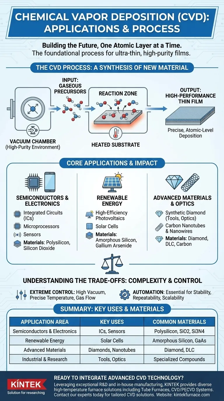
Chemical vapor deposition is a method performed under a highly controlled vacuum, far below atmospheric pressure. The process is not simply a "coating" in the traditional sense; it is a synthesis of new material directly on a surface.
The Deposition Process
A substrate, which is the base material to be coated, is placed inside the vacuum chamber. Gaseous molecules, known as precursors, are then introduced into the chamber.
These precursors react or decompose upon contact with the heated substrate. The chemical reaction leaves behind a solid material, forming a thin, durable film on the substrate's surface, one layer of atoms or molecules at a time.
Achieving Purity and Performance
Because this process occurs in a high-vacuum environment, contamination from the atmosphere is minimized. This results in thin films of extremely high quality and purity, which is critical for applications like microelectronics where even the smallest impurity can cause a device to fail.
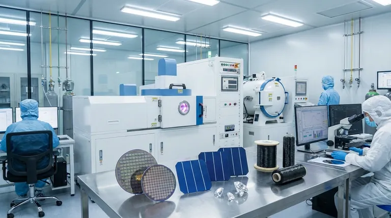
Core Application: The Semiconductor Industry
The most widespread and critical use of CVD is in the manufacturing of semiconductor devices. It is a fundamental step in producing virtually all modern integrated circuits (ICs).
Building Integrated Circuits (ICs)
CVD is used to deposit various materials that form the intricate, layered structures of a microchip. This includes depositing layers of polysilicon, silicon dioxide, and other compounds that act as conductors, insulators, and gates for transistors.
Powering Photovoltaics
The technology is also vital for creating solar cells. CVD is used to deposit films of amorphous polysilicon or other materials like gallium arsenide, which are essential for converting sunlight into electricity efficiently.
Expanding into Advanced Materials and Optics
Beyond conventional semiconductors, specialized CVD techniques enable the creation of materials with unique properties that would be difficult or impossible to produce otherwise.
Synthetic Diamond and Carbon Nanostructures
Microwave plasma CVD systems are specifically designed to "grow" films of polycrystalline or monocrystalline diamond. These synthetic diamond films have applications in industrial cutting tools, optics, and advanced electronics due to their extreme hardness and thermal conductivity.
This same process can be adapted to produce carbon nanotubes and nanowires, materials with extraordinary strength and electrical properties used in research, electronics, and medicine.
A Broad Industrial Footprint
These advanced materials find uses across a surprising range of sectors, including optics, microwave technology, micromechanics, material processing, and even electrochemistry.
Understanding the Trade-offs: The Complexity of CVD
The precision of CVD comes at a cost of complexity. The process requires a significant investment in equipment and strict operational control to achieve the desired results.
The Need for Extreme Control
CVD systems must maintain a high vacuum with very low leakage to prevent contamination. The process is highly sensitive to variables like pressure, gas flow rates, and especially temperature, which often must be measured with high-precision pyrometers at ranges exceeding 2000°C.
Automation is Key
Due to the number of critical variables, modern CVD systems are fully automated. This ensures the stability of the plasma and the precise, repeatable deposition of films, but it also highlights the technical sophistication required to operate and maintain the equipment.
Making the Right Choice for Your Industry
The specific application of CVD depends entirely on the desired outcome, from mass-produced consumer goods to highly specialized research materials.
- If your primary focus is consumer and automotive electronics: CVD is the non-negotiable process for manufacturing the core ICs, sensors, and microprocessors that power smartphones, wearables, and vehicle control systems.
- If your primary focus is renewable energy: CVD is essential for producing the high-efficiency photovoltaic films used in modern solar panels.
- If your primary focus is research and advanced materials: Specialized CVD techniques are the key to developing next-generation materials like synthetic diamonds, carbon nanotubes, and specialized optical coatings.
Ultimately, chemical vapor deposition is less a single application and more a fundamental enabling technology that makes much of our modern world possible.
Summary Table:
| Application Area | Key CVD Uses | Common Materials Deposited |
|---|---|---|
| Semiconductors & Electronics | Manufacturing integrated circuits (ICs), microprocessors, sensors | Polysilicon, Silicon Dioxide, Silicon Nitride |
| Renewable Energy | Production of high-efficiency solar cells (photovoltaics) | Amorphous Silicon, Gallium Arsenide |
| Advanced Materials | Creating synthetic diamonds, carbon nanotubes, optical coatings | Diamond, Carbon Nanotubes, DLC |
| Industrial & Research | Cutting tools, optics, micromechanics, electrochemistry | Various specialized compounds |
Ready to integrate advanced CVD technology into your R&D or production line?
Leveraging exceptional R&D and in-house manufacturing, KINTEK provides diverse laboratories with advanced high-temperature furnace solutions. Our product line, including Tube Furnaces, CVD/PECVD Systems, and Vacuum & Atmosphere Furnaces, is complemented by our strong deep customization capability to precisely meet your unique experimental and production requirements for thin-film deposition.
Contact our experts today to discuss how our tailored CVD solutions can accelerate your project's success.
Visual Guide
Related Products
- Custom Made Versatile CVD Tube Furnace Chemical Vapor Deposition CVD Equipment Machine
- RF PECVD System Radio Frequency Plasma Enhanced Chemical Vapor Deposition
- MPCVD Machine System Reactor Bell-jar Resonator for Lab and Diamond Growth
- 915MHz MPCVD Diamond Machine Microwave Plasma Chemical Vapor Deposition System Reactor
- Slide PECVD Tube Furnace with Liquid Gasifier PECVD Machine
People Also Ask
- What are the key application fields of CVD tube furnaces? Unlock Precision in Thin-Film Synthesis
- What are the benefits of developing new precursor materials for CVD tube furnaces? Unlock Advanced Thin-Film Synthesis
- How does CVD tube furnace sintering enhance graphene growth? Achieve Superior Crystallinity and High Electron Mobility
- Which industries and research fields benefit from CVD tube furnace sintering systems for 2D materials? Unlock Next-Gen Tech Innovations
- What is a CVD tube furnace and what is its primary function? Discover Precision Thin-Film Deposition


