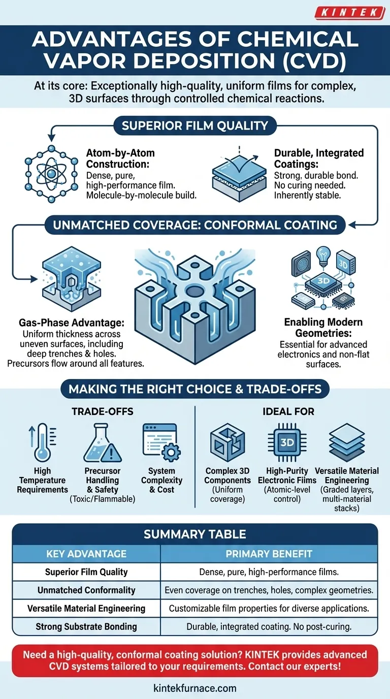
At its core, the primary advantage of Chemical Vapor Deposition (CVD) is its ability to produce exceptionally high-quality, uniform films that conform precisely to complex, three-dimensional surfaces. This is achieved through a chemical reaction of precursor gases on a substrate, resulting in high deposition rates and the versatility to create dynamically layered materials, making it a cornerstone technology in advanced manufacturing.
While many methods can deposit a thin film, they often struggle with quality and coverage on anything but a flat surface. CVD's fundamental advantage is its ability to "grow" a dense, pure, and highly conformal coating from a gas phase, making it indispensable for creating the complex micro-architectures that power modern electronics.
The Foundational Strength: Superior Film Quality
The CVD process is not simply "spraying" material onto a surface; it's a controlled chemical reaction that builds a film molecule-by-molecule. This unique mechanism is the source of its most significant benefits.
Atom-by-Atom Construction
CVD introduces precursor gases into a vacuum chamber, which then decompose and react on the heated substrate. This results in an exceptionally dense, pure, and high-performance film.
This atomic-level control is why CVD is a dominant process in the semiconductor industry, where even the slightest imperfection can render a microchip useless.
Durable, Integrated Coatings
Because the film is formed via a chemical reaction at the surface, it creates a strong, durable bond with the substrate. The resulting coating is inherently stable and requires no subsequent curing, streamlining the manufacturing process.
Unmatched Coverage: Conformal Coating
Perhaps the most celebrated advantage of CVD is its conformality—the ability of the film to maintain a uniform thickness across an uneven surface.
The "Gas-Phase" Advantage
Unlike line-of-sight deposition methods (like Physical Vapor Deposition), CVD precursors exist as a gas that flows into and around any feature on the substrate. The chemical reaction happens everywhere the gas can reach.
This allows CVD to evenly coat the inside of deep trenches, holes, and other complex 3D structures where other methods would fail.
Enabling Modern Geometries
This conformality is not just a minor benefit; it is an enabling technology for countless modern devices.
From automotive sensors and smart home devices to the intricate 3D transistors in your smartphone, CVD makes it possible to build reliable electronic components on non-flat surfaces.
Understanding the Trade-offs
No process is without its challenges. To make an informed decision, you must understand the trade-offs associated with CVD.
High Temperature Requirements
Traditional CVD processes often require very high substrate temperatures (hundreds or even thousands of degrees Celsius) to drive the necessary chemical reactions. This can limit the types of materials that can be used as substrates.
Precursor Handling and Safety
The precursor chemicals used in CVD can be highly toxic, flammable, or corrosive. Implementing a CVD process requires significant investment in safety protocols, gas handling systems, and abatement.
System Complexity and Cost
CVD reactors are sophisticated and expensive pieces of equipment. They operate under vacuum and require precise control over temperature, pressure, and gas flow, representing a significant capital investment.
Making the Right Choice for Your Application
CVD is a powerful and versatile process, but its suitability depends entirely on your end goal.
- If your primary focus is coating complex 3D components: CVD's outstanding conformality is its defining advantage, ensuring uniform coverage in recesses and over sharp edges.
- If your primary focus is creating high-purity electronic films: CVD offers the atomic-level control necessary to produce the high-performance, defect-free layers required for semiconductors and advanced sensors.
- If your primary focus is versatile material engineering: The ability to change precursor gases during deposition allows for the creation of graded layers or multi-material stacks within a single process run.
Ultimately, you choose CVD when the quality, purity, and conformity of your film are critical to the performance of your final product.
Summary Table:
| Key Advantage | Description | Primary Benefit |
|---|---|---|
| Superior Film Quality | Atom-by-atom construction via chemical reaction. | Dense, pure, and high-performance films. |
| Unmatched Conformality | Gas-phase precursors ensure uniform coating on complex 3D surfaces. | Even coverage on trenches, holes, and intricate geometries. |
| Versatile Material Engineering | Ability to create graded layers or multi-material stacks. | Customizable film properties for diverse applications. |
| Strong Substrate Bonding | Film forms via chemical reaction, creating a durable, integrated coating. | No post-deposition curing required. |
Need a high-quality, conformal coating solution for your complex components? KINTEK leverages exceptional R&D and in-house manufacturing to provide advanced CVD systems tailored to your unique requirements. Our expertise in Vacuum & Atmosphere Furnaces and CVD/PECVD Systems, combined with deep customization capabilities, ensures you get a solution that delivers precise, uniform films for your most challenging applications. Contact our experts today to discuss how we can enhance your manufacturing process!
Visual Guide
Related Products
- Custom Made Versatile CVD Tube Furnace Chemical Vapor Deposition CVD Equipment Machine
- RF PECVD System Radio Frequency Plasma Enhanced Chemical Vapor Deposition
- MPCVD Machine System Reactor Bell-jar Resonator for Lab and Diamond Growth
- 915MHz MPCVD Diamond Machine Microwave Plasma Chemical Vapor Deposition System Reactor
- Slide PECVD Tube Furnace with Liquid Gasifier PECVD Machine
People Also Ask
- What future trends are expected in the development of CVD tube furnaces? Discover Smarter, More Versatile Systems
- Why are CVD tube furnace sintering systems indispensable for 2D material research and production? Unlock Atomic-Scale Precision
- How might AI and machine learning enhance CVD tube furnace processes? Boost Quality, Speed, and Safety
- What are the key features of CVD tube furnaces for 2D material processing? Unlock Precision Synthesis for Superior Materials
- What is a CVD tube furnace and what is its primary function? Discover Precision Thin-Film Deposition


