IDBs don't just propagate—they geometrically self-destruct. During high-temperature CVD growth of 3C-SiC, inversion domain boundaries (IDBs) initially travel vertically upward from the heteroepitaxial interface. However, with increasing film thickness and under stable thermal conditions, these boundaries reorient into a zig‑zag pattern along alternating {111} planes. This crystallographic shift forces the IDB segments to bend, eventually close upon themselves, and macroscopically vanish within the first few tens of micrometers.
The core insight is that IDB annihilation is not a passive stop—it’s an active geometric reorganization. The boundaries switch from vertical propagation to a short-segment, {111}-faceted zig‑zag that collapses topology, self-eliminating the defect before it can propagate deeper into the film.
The Initial Propagation Phase
Vertical Propagation from the Interface
When 3C‑SiC nucleates on a non‑native substrate (such as silicon), domain inversion occurs at the interface, seeding IDBs. These planar defects separate regions of opposite crystal polarity. Initially, the IDBs extend straight up through the growing film, following the direction of net growth. This vertical propagation is the classic “columnar” defect mode seen in many heteroepitaxial systems.
Why Vertical Propagation Is Only the First Act
The vertical phase persists only while the film is thin and the boundary energy favors a near‑perpendicular orientation relative to the growth surface. As thickness increases, thermodynamics and kinetics shift. The system gains the opportunity to lower its total free energy by restructuring these boundaries. The driving force for reorientation comes from the same stable, high‑temperature conditions that enable surface diffusion and atomic re‑arrangement.
The Self‑Annihilation Mechanism
Crystallographic Reorientation onto {111} Planes
At a critical thickness—and critically, under stable thermal conditions—the IDBs deviate from their vertical path. They begin to facet onto the {111} planes of the cubic lattice. In 3C‑SiC, the {111} family offers low‑energy boundary configurations. The boundaries now consist of alternating segments on different {111} planes, creating the distinctive zig‑zag microstructure. Each segment becomes extremely short, measuring less than 20 nanometers. This reduction in linear scale is the key that unlocks annihilation.
How Short Zig‑Zag Segments Enable Bending and Closure
The short segment length limits the lateral extent over which polarity mismatch must be accommodated. As adjacent segments on different {111} planes kink, the boundary line curves. Over many such kinks, the IDB can bend back toward itself, forming a closed loop. Topologically, once a boundary loop closes, there is no more “inside versus outside” polarity conflict—the domain inversion is locally resolved. The defect literally annihilates.
Macroscopic Self‑Elimination and Defect Confinement
This closure process is macroscopic: entire IDB networks that started at the interface collapse within the first few tens of micrometers of film growth. The result is a top layer of 3C‑SiC that is virtually free of substrate‑induced inversion domains. The annihilation is “self‑” in the sense that no external intervention, like substrate patterning or impurity addition, is required—only the right thermal and thickness conditions.
Understanding the Trade‑offs and Limitations
Thermal Sensitivity and Process Window
Self‑annihilation depends on stable high‑temperature conditions. If the CVD process experiences thermal fluctuations or if the temperature is too low, the necessary atomic mobility to reorient onto {111} planes may be insufficient. The IDBs may remain vertical and never reach the annihilation stage. This creates a narrow process window that demands tight furnace control.
Thickness Dependence and Not a Perfect Cure
The annihilation mechanism requires a minimum film thickness—typically a few micrometers—before the zig‑zag transition initiates. Below this thickness, the film still contains propagating IDBs. Moreover, while substrate‑induced IDBs are eliminated, other defects (such as stacking faults or microtwins) can still be present. Self‑annihilation addresses only the inversion domain boundaries, not the full spectrum of heteroepitaxial defects.
Competition with Other Defect Evolution
As IDBs reorient, the atomic rearrangement may interact with other defects. There is potential for new stacking faults to form at the kink points, or for the closing boundary loops to leave residual strain. The final defect population is a balance between IDB annihilation and the generation of secondary defects, which can vary with exact growth parameters.
Making the Right Choice for Your Growth Process
The annihilation mechanism is a powerful built‑in defect filter, but leveraging it requires matching your growth strategy to specific device needs.
- If your primary focus is achieving the lowest possible defect density in a thick 3C‑SiC epilayer: Design your process to reach several tens of micrometers of thickness while maintaining an ultra‑stable, high‑temperature profile. This maximizes the probability of complete IDB annihilation before active device layers are formed.
- If your primary focus is growing thin 3C‑SiC films where thickness is limited: Accept that substrate‑induced IDBs will likely persist through the entire film. Plan your device layout to avoid performance‑critical regions directly above high‑defect‑density areas, or use a buffer layer grown under optimized conditions to confine IDBs before growing the active layer.
- If your primary focus is understanding defect evolution in your particular CVD system: Monitor the film morphology and cross‑sectional TEM early in development. Look for the appearance of {111}‑faceted zig‑zag segments as the tell‑tale sign that your thermal conditions are sufficient to trigger self‑annihilation.
Ultimately, the journey of an IDB from vertical invader to self‑closed loop is a remarkable example of how a material’s own crystallography can heal a foundational defect—if you give it the right thermal environment and enough thickness to work with.
Summary Table:
| Process Phase | Boundary Orientation | Microstructure Feature | Driving Mechanism & Requirements |
|---|---|---|---|
| Initial Propagation | Vertical (Columnar) | Near-perpendicular to growth interface | Dominates in thin films near heteroepitaxial interface |
| Reorientation | Zig-Zag along {111} | Short segments (<20 nm) | High surface diffusion under stable high-temperature CVD |
| Self-Annihilation | Closed Loops | Topological defect collapse | Complete elimination within first tens of micrometers |
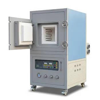
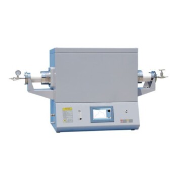
Mastering defect annihilation in 3C-SiC growth requires precise and stable thermal environments. KINTEK specializes in premium laboratory equipment and consumables, offering a comprehensive range of high-temperature furnaces—including customizable CVD, tube, atmosphere, vacuum, and muffle furnaces—designed to meet the rigorous demands of advanced crystal growth and materials research. Enhance your epilayer quality and optimize your thermal process parameters with our expert solutions. Contact KINTEK today to customize your high-temperature furnace system!
Related Products
- HFCVD Machine System Equipment for Drawing Die Nano Diamond Coating
- MPCVD Machine System Reactor Bell-jar Resonator for Lab and Diamond Growth
- 915MHz MPCVD Diamond Machine Microwave Plasma Chemical Vapor Deposition System Reactor
- Custom Made Versatile CVD Tube Furnace Chemical Vapor Deposition CVD Equipment Machine
- RF PECVD System Radio Frequency Plasma Enhanced Chemical Vapor Deposition
People Also Ask
- What is Hot-filament Chemical Vapor Deposition (HFCVD)? Achieve High-Quality Thin Films with Precision Control
- What are the equipment for chemical vapor deposition? A Guide to the 5 Essential Components
- What is the significance of the vacuum pressure control system in the CVD coating process for powders?
- What is the function of high-purity Argon (Ar) gas during CVD? Optimize Your Thin Film Uniformity and Purity
- How do operating temp & pressure in high-temp CVD affect III-nitride MEMS growth? Master 2DEG Epitaxy