The performance of group III-nitride MEMS devices begins at the atomic scale, governed by two primary levers in your high-temperature CVD process: temperature and pressure. For AlGaN/GaN heterostructures—the backbone of countless resonators and sensors—epitaxial growth demands a process temperature near 1120°C and a reduced chamber pressure around 15 mbar. These precise values drive the surface kinetics and gas-phase dynamics needed to deposit an ultra-thin, defect-free barrier layer (e.g., 30 nm AlGaN with 30% aluminum). The direct payoff is a pristine two-dimensional electron gas (2DEG) interface, where high mobility and low sheet resistance determine the MEMS device’s ultimate electrical performance.
Achieving a high-mobility 2DEG in III-nitride MEMS is not just about growing layers; it’s about forging a near-perfect heterojunction. The tandem of high temperature and low pressure is the non-negotiable process foundation that suppresses interfacial defects, ensures crystalline continuity, and preserves the electrical integrity of that critical buried channel.
Why Temperature Is the Architect of Crystal Quality
Setting the Stage for Crystalline Perfection
The substrate temperature directly dictates the phase structure of your III-nitride film. At around 1120°C, adatoms on the growth surface gain sufficient mobility to find their lowest-energy lattice sites. This high surface diffusion length promotes step-flow growth, yielding a fully crystalline, single-phase layer. Lower temperatures produce polycrystalline or amorphous material that is useless for high-performance MEMS.
Balancing Kinetics and Thermodynamics
In the AlGaN/GaN system, this temperature isn’t arbitrary. It must crack ammonia (NH₃) efficiently to supply active nitrogen while enabling trimethylaluminum and triethylgallium to decompose and incorporate without parasitic gas-phase pre-reactions. The high V-III ratio of ~2000 further suppresses nitrogen vacancies, but only if the thermal energy is sufficient to drive the surface reactions. Insufficient heat leads to carbon contamination and vacancy defects that trap charge in the 2DEG.
Preserving the 2DEG Interface
The heterointerface that forms the 2DEG is only a few atomic layers thick. High-temperature growth minimizes interfacial roughness and compositional grading between the AlGaN barrier and the GaN channel. Any disruption here—an atomic step bunch, an unintended diffusion of aluminum—scatters electrons and slashes mobility. Your CVD furnace must therefore deliver multi-zone temperature control with minimal thermal gradient to keep this critical interface perfectly abrupt.
How Low Pressure Perfects Uniformity and Purity
Enhancing Gas Diffusion for Thickness Uniformity
Operating at a reduced pressure of around 15 mbar (1.5 kPa) fundamentally changes the transport of precursor molecules. At atmospheric pressure, gas-phase collisions create stagnant boundary layers and uneven precursor delivery. Lowering chamber pressure dramatically increases the diffusivity of species. This delivers reactants more uniformly across the wafer surface, enabling the deposition of an ultra-thin 30 nm AlGaN barrier with thickness variations measured in single nanometers.
Suppressing Unwanted Gas-Phase Reactions
High-temperature AlGaN growth is plagued by the tendency of precursors to react prematurely in the gas phase, forming particulate clusters that rain down as defects. Low pressure shifts the thermodynamic equilibrium, strongly suppressing these parasitic reactions. The result is a film free of embedded particles that would otherwise pin the 2DEG or degrade MEMS resonator quality factor.
Maintaining a Pristine Growth Environment
A high-vacuum-capable CVD system that reaches very low base pressures minimizes the background partial pressure of oxygen and moisture. At 1120°C, even trace oxygen incorporates into the III-nitride lattice, creating deep-level traps. The combination of low operating pressure and strict vacuum integrity ensures that your 30% aluminum-content barrier layer remains intrinsically pure, preserving the high electric field needed to induce the 2DEG.
The Synergy: Orchestrating the 2DEG
How Temperature and Pressure Work in Unison
Temperature and pressure are not independent knobs; they act in concert to define the deposition regime. At 1120°C and 15 mbar, you enter a mass-transport-limited growth mode where the surface reaction is fast enough to consume all arriving species, yet the low pressure ensures that delivery is uniform and gas-phase nucleation is quenched. This sweet spot is what makes the precise growth of a ternary barrier with tight 30% aluminum composition control possible.
Impact on Electrical Transport
Every parameter tweak shifts the band structure of the heterojunction. Too high a pressure causes thickness non-uniformity that warps the quantum well. Too low a temperature increases carbon impurities that compensate the polarization charge. Your goal—a 2DEG with mobility exceeding 1500 cm²/V·s—is achievable only when both parameters are stabilized within narrow windows, as enabled by a furnace with tight multi-zone temperature control and precise vacuum/pressure regulation.
Understanding the Trade-offs and Pitfalls
Thermal Budget and Substrate Sensitivity
The high process temperature required for AlGaN/GaN is a double-edged sword. It severely restricts your choice of substrates and pre-existing layers. Wafers with dissimilar thermal expansion coefficients may warp or even crack. For heterostructures that include thermally sensitive materials—such as those with pre-deposited metal electrodes—the 1120°C ceiling can be a process-killer, demanding a complex, multi-step protocol.
The Dissociation Danger
At 1120°C, the GaN surface can begin to thermally decompose if the ammonia overpressure is not meticulously maintained. A momentary fluctuation in precursor flow can strip nitrogen atoms from the channel layer, creating vacancy defects right at the heterointerface. This demands that your system’s high-precision mass flow controllers and pressure regulation operate with unwavering stability.
Not a One-Size-Fits-All: The Indium Exception
It’s critical to recognize that this high-temperature regime applies to aluminum-containing nitride alloys. If your MEMS design incorporates InAlN or InGaN layers, you must drop the temperature significantly—often to the 800–900°C range—to prevent indium desorption. The high-temperature equipment that works beautifully for AlGaN may be entirely unsuitable for an indium-bearing process, requiring a different furnace or a carefully managed temperature ramp.
The Cost of Low-Pressure Excellence
Operating at 15 mbar demands a sophisticated vacuum system with fast pumping and clean, dry-pumping technology. A standard tube furnace without vacuum capability cannot deliver the required film uniformity or purity. The investment in equipment and maintenance is higher, but the alternative is an unacceptably defective 2DEG and non-functional MEMS.
Making the Right Choice for Your MEMS Goal
Your process parameters must align with the specific functional demands of your MEMS device. Use the following priorities as a design compass, always referencing the 1120°C / 15 mbar baseline for AlGaN/GaN heterostructures:
- If your primary focus is maximizing 2DEG carrier mobility: Anchor your process firmly at 1120°C and 15 mbar. Prioritize a multi-zone furnace with temperature deviation below ±1°C and a V-III ratio above 1500. Invest in a high-vacuum-capable system to eliminate background impurities that act as scattering centers.
- If your primary focus is sub-nanometer thickness uniformity across a large wafer: A low operating pressure (~15 mbar) is your most powerful tool. Select a CVD system with superior chamber geometry and gas injection designed to eliminate recirculation zones, ensuring the boundary layer is uniformly thin.
- If your MEMS stack includes thermally sensitive materials or substrates: You are facing a serious conflict with the baseline III-nitride growth. Investigate lower-temperature buffer layer technologies or shift your design toward an indium-containing heterostructure (e.g., InAlN/GaN), which can be grown at 800–900°C, willingly trading off some thermal stability for process compatibility.
- If your goal is to minimize defect density for a high-Q resonator: Focus not only on temperature magnitude but on the ramp and cooldown rates. A CVD furnace with exceptional thermal uniformity will prevent stress-induced misfit dislocations at the heterointerface, directly preserving the resonance quality factor.
Your MEMS device lives or dies by the first few atomic layers of its heterostructure. By wielding the full precision of high-temperature, low-pressure CVD, you are not just growing a film—you are engineering the electrical heart of your device.
Summary Table:
| Process Parameter | Optimal Target | Primary Function & Impact | Impact on 2DEG / MEMS Performance |
|---|---|---|---|
| Substrate Temperature | ~1120°C | Promotes step-flow growth, efficient precursor decomposition, and high adatom mobility | Minimizes interfacial roughness and defects; preserves electron mobility |
| Chamber Pressure | ~15 mbar (1.5 kPa) | Enhances gas diffusivity and suppresses parasitic gas-phase reactions | Enables nanometer-scale thickness uniformity and particle-free films |
| V-III Ratio & Vacuum | ~2000 Ratio; High Vacuum | Suppresses nitrogen vacancies and background contaminants ($O_2$, $H_2O$) | Yields high 2DEG carrier mobility (>1500 cm²/V·s) and low sheet resistance |
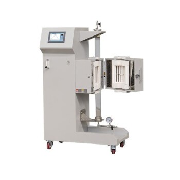
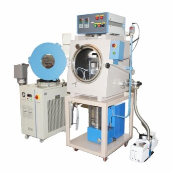
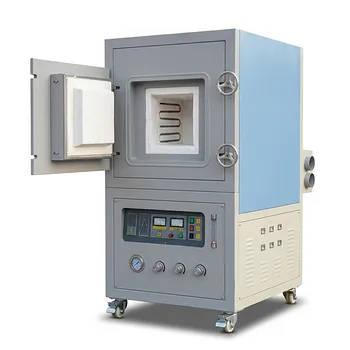
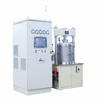
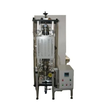
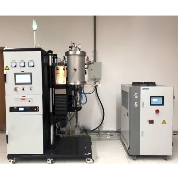
Ready to achieve pristine 2DEG interfaces and defect-free epitaxy for your III-nitride MEMS devices? KINTEK specializes in advanced laboratory equipment and consumables, offering a comprehensive range of high-temperature furnaces—including specialized CVD, vacuum, tube, muffle, atmosphere, rotary, dental, and induction melting furnaces—all fully customizable to satisfy your unique process requirements. Whether you need multi-zone thermal precision within ±1°C or stringent vacuum and pressure regulation, our tailor-made systems empower you to eliminate interfacial defects and boost device performance. Contact KINTEK today to consult with our thermal equipment experts and design your ideal high-temperature CVD furnace solution!
Related Products
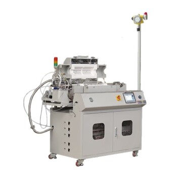
- Custom Made Versatile CVD Tube Furnace Chemical Vapor Deposition CVD Equipment Machine
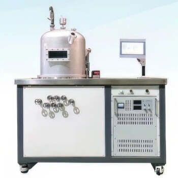
- HFCVD Machine System Equipment for Drawing Die Nano Diamond Coating
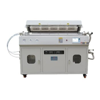
- Multi Heating Zones CVD Tube Furnace Machine for Chemical Vapor Deposition Equipment
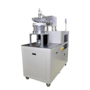
- MPCVD Machine System Reactor Bell-jar Resonator for Lab and Diamond Growth
- 915MHz MPCVD Diamond Machine Microwave Plasma Chemical Vapor Deposition System Reactor
People Also Ask
- What is a CVD tube furnace and what is its primary function? Discover Precision Thin-Film Deposition
- Why are CVD tube furnace sintering systems indispensable for 2D material research and production? Unlock Atomic-Scale Precision
- How does CVD tube furnace sintering enhance graphene growth? Achieve Superior Crystallinity and High Electron Mobility
- Which industries and research fields benefit from CVD tube furnace sintering systems for 2D materials? Unlock Next-Gen Tech Innovations
- What future trends are expected in the development of CVD tube furnaces? Discover Smarter, More Versatile Systems