In short, the industries and research fields that benefit most from CVD tube furnace systems for 2D materials are those pioneering next-generation technology. This includes semiconductor manufacturing, energy storage like Li-ion batteries and supercapacitors, flexible electronics, optoelectronics, photocatalysis, and advanced sensor development. These systems provide the highly controlled environment required to synthesize and refine materials that are only a single atom thick.
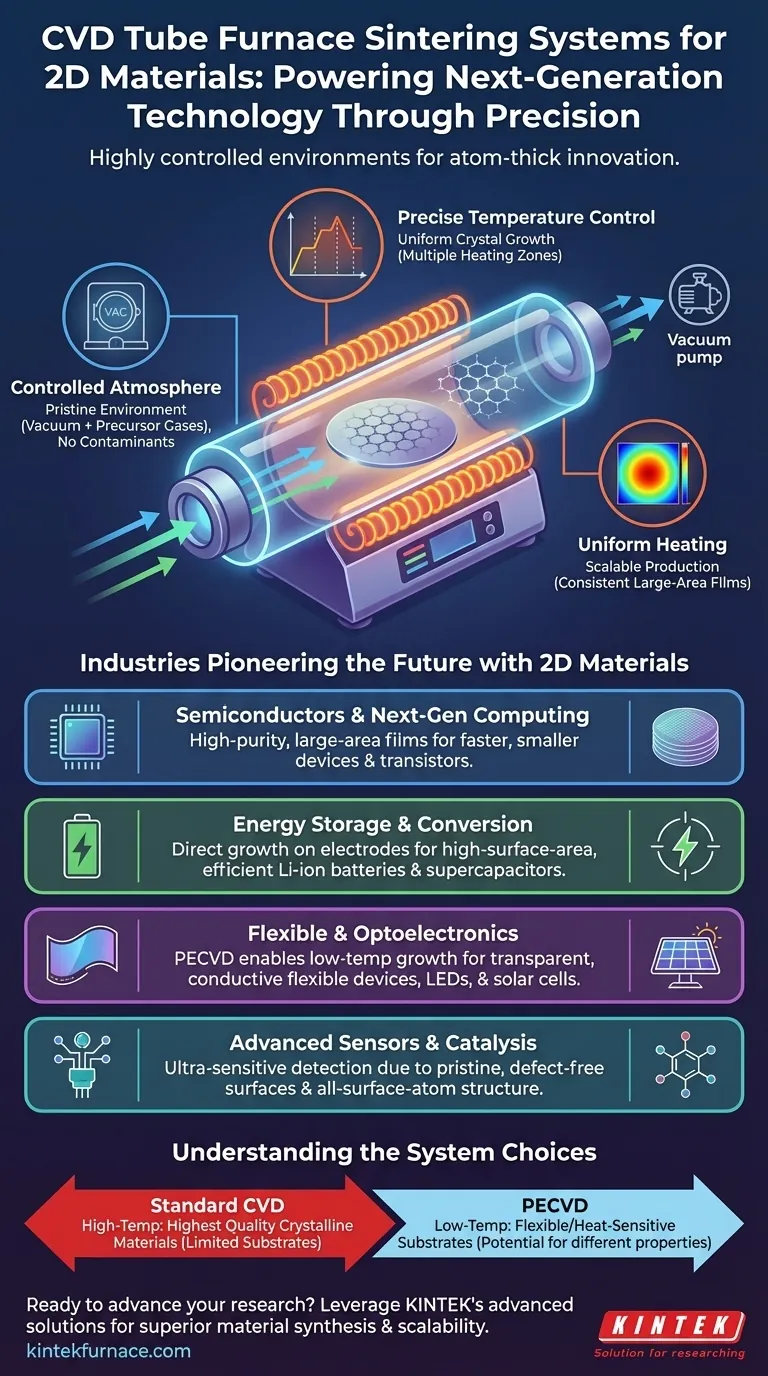
A CVD tube furnace is not just a high-temperature oven; it is a precision instrument. Its value lies in its ability to create a pristine, highly controlled environment, which is the absolute prerequisite for fabricating the uniform, defect-free 2D materials needed to unlock their revolutionary electronic and physical properties.
Why CVD Furnaces Are Essential for 2D Materials
Synthesizing a material like graphene or a transition metal dichalcogenide (TMD) is a process of atomic-level construction. Chemical Vapor Deposition (CVD) is the leading method for this, and the tube furnace is the environment where it happens. The furnace's specific capabilities are what make high-quality 2D material growth possible.
The Need for a Controlled Atmosphere
To build a perfect atomic layer, you must control exactly which atoms are present. A CVD furnace is sealed to create a vacuum, removing all contaminants.
Then, specific precursor gases are introduced in precise amounts. This controlled atmosphere ensures that only the desired chemical reactions occur on the substrate, preventing unwanted impurities and structural defects in the 2D material lattice.
The Critical Role of Temperature Control
Temperature dictates the rate of chemical reactions and the quality of crystal growth. Too low, and the reaction won't proceed; too high, and it can cause defects or damage the substrate.
CVD furnaces offer precise temperature control, often with multiple heating zones. This allows researchers to create specific temperature profiles that are essential for nucleating and growing large, uniform, single-layer films.
Uniform Heating for Scalable Production
For a 2D material to be useful in a device like a transistor or a sensor, it must be consistent across its entire surface.
A tube furnace is designed to provide highly uniform heating over the entire substrate area. This uniformity is critical for moving from lab-scale curiosities to producing wafers that can be used in industrial fabrication.
Key Applications and Benefitting Fields
The precise control offered by CVD furnace systems directly enables breakthroughs in several high-tech fields.
Semiconductors and Next-Gen Computing
The semiconductor industry is constantly pushing to make transistors smaller and faster. 2D materials like graphene and MoS₂ offer incredible electron mobility in an atomically thin form factor. CVD is the primary method for producing the high-purity, large-area films needed for wafer-scale fabrication.
Energy Storage and Conversion
The performance of batteries and supercapacitors depends heavily on the surface area of the electrode material. 2D materials have the highest possible surface-area-to-volume ratio. CVD can be used to grow these materials directly onto conductive foils, creating highly efficient electrodes for next-generation Li-ion batteries and supercapacitors.
Flexible and Optoelectronic Devices
2D materials are both transparent and conductive, making them ideal for touch screens, flexible displays, LEDs, and solar cells. Many flexible substrates, like polymers, cannot withstand the high temperatures of traditional CVD.
This has driven the adoption of specialized techniques like Plasma-Enhanced CVD (PECVD). PECVD systems operate at lower temperatures, enabling the direct, transfer-free growth of 2D materials onto heat-sensitive substrates.
Advanced Sensors and Catalysis
Because every atom in a 2D material is a surface atom, they are exceptionally sensitive to their surrounding environment. This makes them perfect for building ultra-sensitive chemical and biological sensors.
The pristine and clean surfaces produced via CVD are essential for ensuring that the sensor responds only to the target analyte without interference from surface contaminants.
Understanding the Trade-offs
While indispensable, CVD furnace systems are not a one-size-fits-all solution. Understanding their variations and limitations is key to successful implementation.
Standard CVD vs. Plasma-Enhanced CVD (PECVD)
Standard thermal CVD relies purely on high temperatures to drive reactions. It typically produces the highest-quality crystalline materials but is limited to temperature-resistant substrates.
PECVD uses a plasma to energize the precursor gases, allowing deposition to occur at much lower temperatures. This is a key advantage for flexible electronics but may sometimes result in material with different properties or more defects than high-temperature growth.
The Challenge of Material Transfer
Often, a 2D material is grown on a catalytic substrate (like copper for graphene) and must be transferred to a final device substrate (like silicon). This transfer process is a major source of defects, wrinkles, and contamination that can degrade device performance.
The development of transfer-free processes, often enabled by PECVD, where the material is grown directly on the final non-catalytic substrate, is a significant area of research aimed at overcoming this hurdle.
Cost and Industrial Scalability
CVD furnace systems, especially those with advanced capabilities, represent a significant investment. While they are a cornerstone of research and development, scaling these processes for high-volume, low-cost industrial manufacturing remains a major engineering challenge.
Making the Right Choice for Your Goal
Your application's specific requirements will determine the type of CVD system and process you need.
- If your primary focus is fundamental research: You require a system with maximum control over temperature, gas flow, and purity to produce novel, pristine materials with the highest possible quality.
- If your primary focus is semiconductor fabrication: You need a system that prioritizes uniformity, repeatability, and compatibility with large-area wafers.
- If your primary focus is flexible electronics: You must use a system capable of low-temperature deposition, such as PECVD, to avoid damaging your polymer substrates.
- If your primary focus is energy storage: You need a process that can effectively grow high-surface-area 2D materials directly onto conductive electrode structures.
Mastering the synthesis environment is the fundamental key to unlocking the vast potential of 2D materials.
Summary Table:
| Field/Industry | Key Applications | CVD Furnace Benefits |
|---|---|---|
| Semiconductors | Next-gen computing, transistors | High-purity, large-area films, precise temperature control |
| Energy Storage | Li-ion batteries, supercapacitors | Direct growth on electrodes, high surface area |
| Flexible Electronics | Touch screens, displays, LEDs | Low-temperature PECVD for heat-sensitive substrates |
| Optoelectronics | Solar cells, sensors | Uniform heating, defect-free surfaces |
| Catalysis & Sensors | Chemical/biological detection | Clean surfaces, controlled atmosphere |
Ready to advance your 2D material research with precision? Leveraging exceptional R&D and in-house manufacturing, KINTEK provides diverse laboratories with advanced high-temperature furnace solutions. Our product line, including Muffle, Tube, Rotary Furnaces, Vacuum & Atmosphere Furnaces, and CVD/PECVD Systems, is complemented by our strong deep customization capability to precisely meet unique experimental requirements. Whether you're in semiconductors, energy storage, or flexible electronics, we can help you achieve superior material synthesis and scalability. Contact us today to discuss how our tailored solutions can drive your innovations forward!
Visual Guide
Related Products
- Custom Made Versatile CVD Tube Furnace Chemical Vapor Deposition CVD Equipment Machine
- Split Chamber CVD Tube Furnace with Vacuum Station CVD Machine
- Multi Heating Zones CVD Tube Furnace Machine for Chemical Vapor Deposition Equipment
- Slide PECVD Tube Furnace with Liquid Gasifier PECVD Machine
- Inclined Rotary Plasma Enhanced Chemical Deposition PECVD Tube Furnace Machine
People Also Ask
- What is a CVD tube furnace and what is its primary function? Discover Precision Thin-Film Deposition
- How can integrating CVD tube furnaces with other technologies benefit device fabrication? Unlock Advanced Hybrid Processes
- How might AI and machine learning enhance CVD tube furnace processes? Boost Quality, Speed, and Safety
- What future trends are expected in the development of CVD tube furnaces? Discover Smarter, More Versatile Systems
- Why are CVD tube furnace sintering systems indispensable for 2D material research and production? Unlock Atomic-Scale Precision