In short, sintering within a Chemical Vapor Deposition (CVD) tube furnace is a critical high-temperature step that transforms deposited carbon atoms into a high-quality graphene film. This process uses thermal energy to rearrange the atoms into a more perfect crystalline structure, removing defects and improving the material's electrical properties.
The true function of the CVD furnace and subsequent sintering is to provide a highly controlled environment—first for the precise deposition of carbon, and second for the thermal refinement that "heals" the resulting film into a near-perfect atomic sheet.
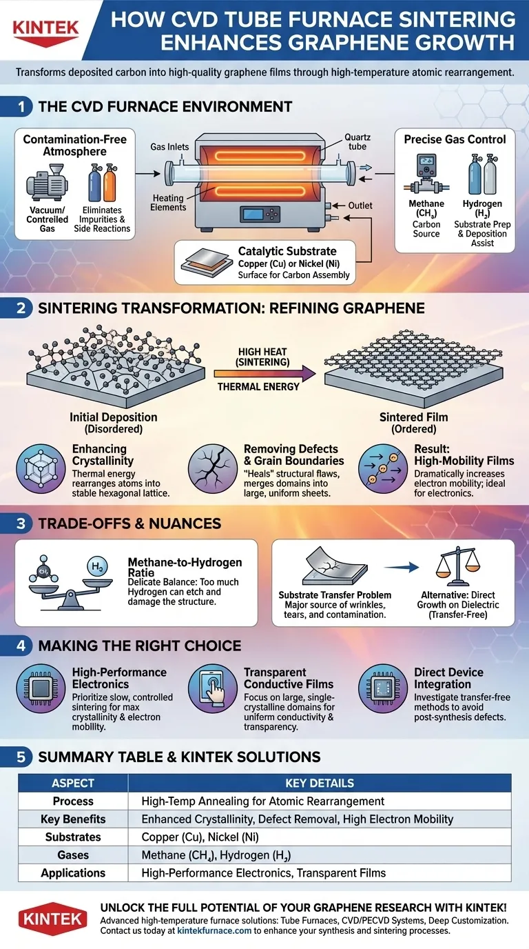
The Role of the CVD Furnace Environment
To understand sintering, you must first understand the environment the CVD furnace creates. It is a system designed for extreme precision at the atomic level.
A Contamination-Free Atmosphere
The process begins by creating a vacuum or filling the furnace tube with a specific, controlled gas mixture. This eliminates impurities and prevents unwanted side reactions that could introduce flaws into the graphene lattice.
The Catalytic Substrate
Graphene growth via CVD typically occurs on a catalytic metal substrate, most commonly copper (Cu) or nickel (Ni). This substrate acts as the surface upon which carbon atoms from the gas phase will assemble.
Precise Gas Control
The furnace allows for the precise control of precursor gases. Methane (CH₄) is commonly used as the carbon source, while hydrogen (H₂) is used to prepare the substrate and assist in the uniform deposition of carbon.
How Sintering Transforms the Graphene
Sintering is the high-temperature annealing phase that follows the initial deposition of carbon. This is where the material is fundamentally refined.
Enhancing Crystallinity
The high heat of the sintering process provides thermal energy to the deposited carbon atoms. This energy allows them to move and rearrange themselves from a disordered state into the stable hexagonal lattice characteristic of graphene, significantly enhancing crystallinity.
Removing Defects and Grain Boundaries
During initial growth, imperfections and boundaries between different crystalline domains can form. Sintering helps to "heal" these structural defects and merge smaller domains into larger, more uniform single-crystal sheets.
The Result: High-Mobility Films
The direct result of improved crystallinity and fewer defects is a dramatic increase in electron mobility. Electrons can travel across the graphene sheet with far less scattering, making the material ideal for high-performance electronics and transparent conductive electrodes.
Understanding the Trade-offs and Nuances
Achieving high-quality graphene is not automatic. It requires navigating critical process parameters and understanding the inherent challenges.
The Methane-to-Hydrogen Ratio
The balance between methane and hydrogen is delicate. While hydrogen helps prepare the surface for growth, too much hydrogen can act as an etchant, corroding and damaging the very graphene structure you are trying to create.
The Substrate Transfer Problem
For most electronic applications, the graphene grown on a metal foil must be transferred to a dielectric substrate. This transfer process is a major source of wrinkles, tears, and contamination, potentially undoing the quality gained during synthesis.
Transfer-Free Alternatives
To bypass this issue, methods like gaseous catalyst-assisted CVD are being developed. These aim to grow high-quality graphene directly on dielectric substrates, eliminating the damaging transfer step entirely.
Making the Right Choice for Your Goal
The specific parameters of your CVD and sintering process depend entirely on the desired end-product.
- If your primary focus is high-performance electronics: Prioritize a slow, controlled sintering process to maximize crystallinity and achieve the highest possible electron mobility.
- If your primary focus is transparent conductive films: Focus on conditions that promote large, single-crystalline domains to ensure uniform conductivity and transparency over large areas.
- If your primary focus is direct device integration: Investigate transfer-free growth methods to avoid the defects and contamination introduced by post-synthesis handling.
Ultimately, mastering the furnace environment gives you direct control over the final quality and properties of your graphene film.
Summary Table:
| Aspect | Key Details |
|---|---|
| Process | High-temperature annealing in CVD furnace for atomic rearrangement |
| Key Benefits | Enhanced crystallinity, defect removal, increased electron mobility |
| Common Substrates | Copper (Cu), Nickel (Ni) |
| Gases Used | Methane (CH₄), Hydrogen (H₂) |
| Applications | High-performance electronics, transparent conductive films |
Unlock the full potential of your graphene research with KINTEK's advanced high-temperature furnace solutions! Leveraging exceptional R&D and in-house manufacturing, we provide diverse laboratories with tailored options like Tube Furnaces, CVD/PECVD Systems, and more. Our strong deep customization capability ensures precise alignment with your unique experimental needs, whether you're focusing on high electron mobility, large-area films, or direct device integration. Contact us today to discuss how our expertise can enhance your graphene synthesis and sintering processes for superior results!
Visual Guide
Related Products
- Custom Made Versatile CVD Tube Furnace Chemical Vapor Deposition CVD Equipment Machine
- Split Chamber CVD Tube Furnace with Vacuum Station CVD Machine
- Multi Heating Zones CVD Tube Furnace Machine for Chemical Vapor Deposition Equipment
- Slide PECVD Tube Furnace with Liquid Gasifier PECVD Machine
- Inclined Rotary Plasma Enhanced Chemical Deposition PECVD Tube Furnace Machine
People Also Ask
- What is a CVD tube furnace and what is its primary function? Discover Precision Thin-Film Deposition
- What are the key application fields of CVD tube furnaces? Unlock Precision in Thin-Film Synthesis
- How might AI and machine learning enhance CVD tube furnace processes? Boost Quality, Speed, and Safety
- Why are CVD tube furnace sintering systems indispensable for 2D material research and production? Unlock Atomic-Scale Precision
- What customization options are available for CVD tube furnaces? Tailor Your System for Superior Material Synthesis