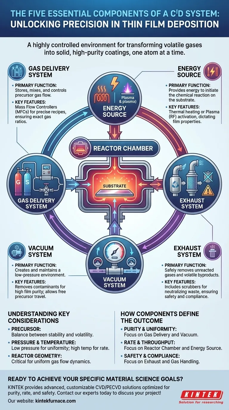
At its core, a Chemical Vapor Deposition (CVD) system is a highly controlled environment designed for a specific task: depositing exceptionally thin films of material onto a substrate. A complete CVD apparatus is comprised of five essential equipment groups: a gas delivery system, a reactor chamber, an energy source, a vacuum system, and an exhaust system. Each component plays a precise role in transforming volatile chemical gases into a solid, high-purity coating.
A CVD system is not merely a collection of hardware. It is a precisely engineered process where each component works in concert to transport volatile chemicals into a vacuum, provide the energy for them to react, and uniformly deposit a new layer of material, one atom or molecule at a time.
The Anatomy of a CVD System
To understand CVD, you must first understand the function of each piece of equipment. The process flows logically from gas delivery to final exhaust, with the reaction occurring at the center.
The Gas Delivery System
This system is the starting point of the entire process. Its job is to store, mix, and precisely control the flow rate of the chemical precursors into the reactor.
Precursors are the volatile gases or vaporized liquids that contain the elements you wish to deposit. The gas delivery system uses mass flow controllers (MFCs) to ensure the exact recipe of gases enters the chamber at the correct rate.
The Reactor Chamber
The reactor is the heart of the CVD system. It is a sealed chamber designed to contain the reaction and house the material being coated, known as the substrate.
The chamber's design is critical for ensuring the gases flow uniformly over the substrate, which directly impacts the evenness and quality of the final thin film.
The Energy Source
Chemical vapor deposition requires energy to break down the precursor gases and initiate the chemical reaction on the substrate surface. This energy can be supplied in several forms.
Common methods include thermal energy, where the substrate is heated to high temperatures, or plasma energy, where an electromagnetic field (like a radio frequency or RF field) energizes the gas into a reactive plasma state. The choice of energy source dictates the process parameters and the types of films that can be grown.
The Vacuum System
CVD is performed under vacuum, at pressures well below our normal atmosphere. The vacuum system, typically a series of pumps, is responsible for creating and maintaining this low-pressure environment.
First, it removes air and any other contaminant particles from the reactor chamber, ensuring high film purity. Second, the low pressure allows the precursor molecules to travel freely to the substrate surface without colliding with other gas molecules.
The Exhaust System
Once the reaction is complete, not all precursor gases will have been consumed. The exhaust system safely removes these unreacted gases and any volatile byproducts from the chamber.
This is a critical safety and environmental component, as many precursor chemicals can be toxic, flammable, or harmful. The exhaust often includes "scrubbers" or abatement systems that neutralize the waste gases before they are released.
Understanding Key System Considerations
The performance of a CVD system is determined by the interplay between its components. Simply having all the parts is not enough; they must be optimized for a specific outcome, which always involves trade-offs.
Precursor Stability vs. Volatility
The chemicals used in CVD must be volatile enough to be transported as a gas but stable enough not to decompose before reaching the substrate. This balance is fundamental. An overly stable precursor requires too much energy to react, while an unstable one can clog the gas lines or deposit film in unwanted areas.
Pressure and Temperature Control
The vacuum system and energy source are in a constant partnership. The pressure inside the reactor determines how molecules move, while the temperature provides the energy for the reaction. A lower pressure might improve film uniformity but decrease the deposition rate. Higher temperatures can increase the rate but may also damage a sensitive substrate.
Reactor Geometry
The shape and size of the reactor chamber are not arbitrary. The design dictates the flow dynamics of the gases inside. A poor design can lead to turbulence or stagnant zones, resulting in a film that is thicker in some areas and thinner in others, compromising the device's performance.
How Each Component Defines the Outcome
When designing or choosing a CVD process, your primary goal will dictate which components require the most attention.
- If your primary focus is film purity and uniformity: Your gas delivery and vacuum systems are paramount for preventing contamination and ensuring even gas flow.
- If your primary focus is deposition rate and throughput: The design of your reactor chamber and the power of your energy source will be the main factors limiting your speed.
- If your primary focus is safety and environmental compliance: The exhaust and gas handling systems require the most rigorous design, monitoring, and maintenance protocols.
Ultimately, understanding how these distinct equipment systems interact is the key to mastering the CVD process and achieving your specific material science goals.
Summary Table:
| Component | Primary Function | Key Features |
|---|---|---|
| Gas Delivery System | Stores, mixes, and controls precursor gas flow | Mass Flow Controllers (MFCs) for precise recipes |
| Reactor Chamber | Houses the substrate for the deposition reaction | Sealed design for uniform gas flow and film quality |
| Energy Source | Provides energy to initiate the chemical reaction | Thermal heating or Plasma (RF) activation |
| Vacuum System | Creates and maintains a low-pressure environment | Removes contaminants, ensures high film purity |
| Exhaust System | Safely removes unreacted gases and byproducts | Scrubbers for safety and environmental compliance |
Ready to Achieve Your Specific Material Science Goals?
Understanding the theory is the first step; implementing it requires a system perfectly tailored to your unique experimental requirements. KINTEK specializes in providing advanced, high-performance CVD solutions for diverse laboratories.
Leveraging our exceptional R&D and in-house manufacturing capabilities, we offer a comprehensive product line—including sophisticated CVD/PECVD Systems—complemented by strong deep customization. We ensure your system is optimized for your primary focus, whether it's ultimate film purity, high deposition rate, or stringent safety compliance.
Let's build your ideal CVD process together. Contact our experts today to discuss your project and discover the KINTEK difference.
Visual Guide
Related Products
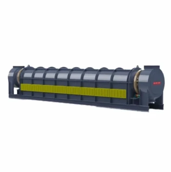
- Custom Made Versatile CVD Tube Furnace Chemical Vapor Deposition CVD Equipment Machine
- HFCVD Machine System Equipment for Drawing Die Nano Diamond Coating
- Multi Heating Zones CVD Tube Furnace Machine for Chemical Vapor Deposition Equipment
- MPCVD Machine System Reactor Bell-jar Resonator for Lab and Diamond Growth
- 915MHz MPCVD Diamond Machine Microwave Plasma Chemical Vapor Deposition System Reactor
People Also Ask
- What is a CVD tube furnace and what is its primary function? Discover Precision Thin-Film Deposition
- How might AI and machine learning enhance CVD tube furnace processes? Boost Quality, Speed, and Safety
- How can integrating CVD tube furnaces with other technologies benefit device fabrication? Unlock Advanced Hybrid Processes
- What are the key application fields of CVD tube furnaces? Unlock Precision in Thin-Film Synthesis
- How does CVD tube furnace sintering enhance graphene growth? Achieve Superior Crystallinity and High Electron Mobility