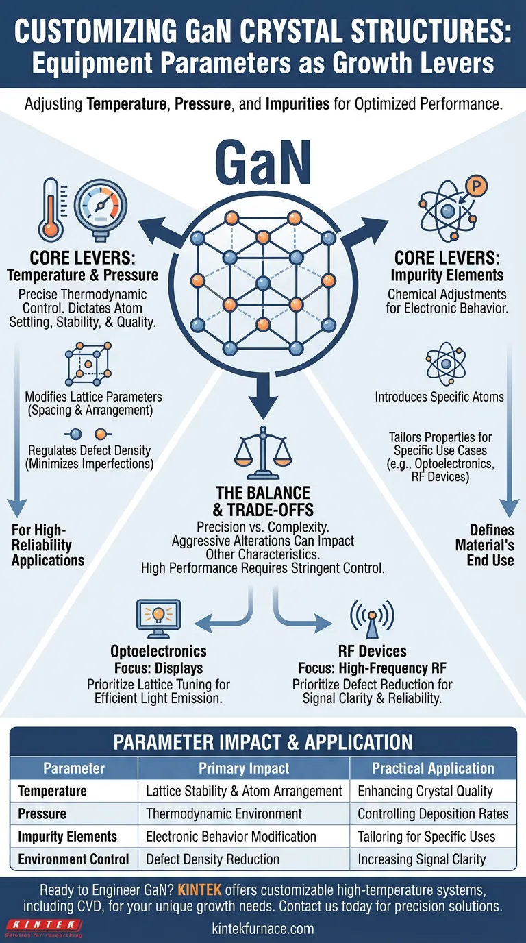
The physical characteristics of Gallium Nitride (GaN) crystal structures can be directly manipulated by adjusting three specific parameters within the growth equipment: temperature, pressure, and the introduction of impurity elements. By fine-tuning these variables, engineers can alter the material's lattice parameters and control the density of defects, effectively customizing the crystal for specific performance requirements.
By precisely regulating the growth environment, the standard wurtzite structure of GaN can be engineered to meet distinct industrial needs. This control over lattice dimensions and defect rates is the key factor that allows GaN to serve in applications as varied as optoelectronic displays and high-frequency radio frequency (RF) devices.
The Core Levers of Growth Control
Regulating Temperature and Pressure
The primary method for adjusting GaN characteristics involves the precise control of the thermodynamic environment inside the deposition equipment.
Temperature and pressure act as the fundamental "knobs" during the growth process. These settings dictate how atoms settle into the crystal lattice, influencing the overall stability and quality of the final material.
Modifying Lattice Parameters
The internal architecture of GaN is typically a wurtzite structure.
By shifting growth conditions, you can adjust the lattice parameters—essentially the spacing and arrangement of atoms within this structure. This tuning is critical for ensuring the material integrates well with other substrates or layers in a device stack.
Managing Defect Density
No crystal growth process is perfectly uniform; irregularities known as defects inevitably occur.
However, the density of these defects is not random. It is a direct result of the chosen equipment parameters. Tighter control over the growth environment allows you to minimize these imperfections, which is essential for high-reliability applications.
Chemical Adjustments via Impurities
Introducing Specific Elements
Beyond simple thermodynamic controls, the physical properties of GaN are adjusted by introducing specific impurity elements during growth.
This process is deliberate. By adding foreign atoms into the crystal matrix, you modify the material's electronic behavior without destroying its structural integrity.
Tailoring for Specific Applications
The combination of physical (temperature/pressure) and chemical (impurities) adjustments is what defines the material's end use.
For example, a GaN crystal grown for an optoelectronic display requires a different recipe than one grown for a high-frequency RF device. The equipment parameters serve as the bridge between raw materials and these specialized functions.
Understanding the Trade-offs
The Balance of Precision
Achieving the ideal lattice structure often requires a delicate balance.
Aggressively altering parameters to fix one characteristic, such as lattice spacing, can inadvertently impact another, such as defect density.
Complexity vs. Performance
High-performance devices generally demand lower defect densities and precise lattice matching.
Achieving this level of precision typically requires more stringent control over the equipment, potentially increasing the complexity of the manufacturing process.
Making the Right Choice for Your Goal
To optimize Gallium Nitride for your specific project, you must align your equipment settings with your performance targets.
- If your primary focus is Optoelectronics (Displays): Prioritize growth parameters and impurity profiles that tune the lattice structure for efficient light emission.
- If your primary focus is High-Frequency RF Devices: Focus on environmental controls (temperature and pressure) that minimize defect density to ensure signal clarity and reliability.
Success in GaN fabrication relies on viewing temperature, pressure, and impurities not just as settings, but as tools to engineer the wurtzite structure at the atomic level.
Summary Table:
| Parameter | Primary Impact on GaN | Practical Application |
|---|---|---|
| Temperature | Atom arrangement & lattice stability | Enhancing crystal quality for high-performance devices |
| Pressure | Thermodynamic growth environment | Controlling deposition rates and material uniformity |
| Impurity Elements | Electronic behavior modification | Tailoring crystals for optoelectronics vs. RF electronics |
| Environment Control | Defect density reduction | Increasing reliability for high-frequency signal clarity |
Precision is the foundation of high-performance semiconductor fabrication. Backed by expert R&D and manufacturing, KINTEK offers specialized high-temperature systems including Muffle, Tube, Rotary, Vacuum, and CVD systems—all fully customizable to meet your unique Gallium Nitride (GaN) growth needs. Whether you are aiming for minimal defect density in RF devices or optimized lattice structures for optoelectronics, our equipment provides the exact temperature and pressure control required for success. Contact KINTEK today to discuss your custom furnace requirements!
Visual Guide
References
- Qingyuan Yu. Comparative Analysis of Sic and Gan: Third-Generation Semiconductor Materials. DOI: 10.54097/2q3qyj85
This article is also based on technical information from Kintek Furnace Knowledge Base .
Related Products
- Cylindrical Resonator MPCVD Machine System for Lab Diamond Growth
- MPCVD Machine System Reactor Bell-jar Resonator for Lab and Diamond Growth
People Also Ask
- What factors influence the quality of diamond deposition in the MPCVD method? Master the Critical Parameters for High-Quality Diamond Growth
- What are future trends in MPCVD technology? Unlock Next-Gen Materials with AI and Efficiency
- Why is temperature control important in the MPCVD growth process? Ensure High-Quality, Reliable Diamond Film Deposition
- What technological trend has emerged in MPCVD systems regarding power sources? Shift to Solid-State RF for Precision
- What is the MPCVD method and why is it considered effective for diamond deposition? Superior Purity & High Growth Rates

