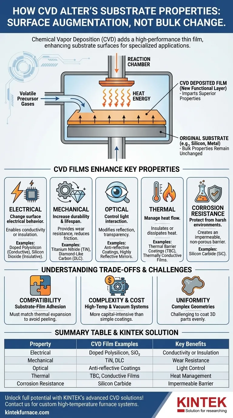
In essence, the Chemical Vapor Deposition (CVD) process fundamentally enhances a substrate by depositing a new, high-performance thin film onto its surface. Rather than changing the bulk material itself, CVD adds a functional layer that imparts superior electrical, mechanical, optical, thermal, and corrosion-resistance properties, turning a standard component into a specialized one.
The core value of CVD is not in altering the original substrate, but in strategically combining the substrate's bulk properties (like cost, weight, or shape) with the superior surface properties of a deposited film. This allows you to achieve performance characteristics that neither material could offer alone.
The Core Principle: Augmenting the Surface
Chemical Vapor Deposition is a powerful technique used to grow high-purity, solid materials on a surface. Understanding its fundamental mechanism is key to grasping how it enhances properties.
What is Chemical Vapor Deposition (CVD)?
The process involves introducing one or more volatile precursor gases into a reaction chamber containing the substrate. Energy, typically in the form of heat, is applied to trigger a chemical reaction. This reaction causes a solid material to deposit and bond with the substrate, creating a thin, uniform film across its surface.
The Substrate as a Foundation
The substrate serves as the physical foundation for this new layer. Its own properties are not chemically changed. Instead, the final component's performance becomes a composite of the substrate's bulk characteristics and the specialized properties of the new surface film.
How CVD Films Enhance Key Properties
The true power of CVD lies in its versatility. By selecting different precursor gases, you can deposit films that are engineered to solve specific problems.
Enhancing Electrical Properties
A film deposited by CVD can completely change the electrical behavior of a substrate's surface. It can be used to lay down a highly conductive layer, such as doped polysilicon, or a superior insulating layer, like silicon dioxide. This is the foundational process for manufacturing modern microelectronics.
Improving Mechanical Durability
To increase a component's lifespan, CVD is used to apply exceptionally hard coatings like titanium nitride (TiN) or diamond-like carbon (DLC). These films provide a wear-resistant surface that dramatically reduces friction and protects the softer substrate underneath from abrasion and physical damage.
Modifying Optical Characteristics
CVD gives you precise control over how a surface interacts with light. You can deposit films that act as anti-reflective coatings on lenses, create highly reflective surfaces for mirrors, or control the transparency of a material for applications like solar cells and sensors.
Managing Thermal Performance
For components operating at extreme temperatures, CVD can apply a thermal barrier coating (TBC). These ceramic films insulate the underlying substrate, protecting it from heat damage, a critical function in jet engines and gas turbines. Conversely, thermally conductive films can be used to help dissipate heat away from sensitive electronics.
Boosting Corrosion Resistance
A key advantage of CVD is its ability to produce dense, non-porous films. By coating a reactive substrate with an inert material, such as silicon carbide, you create an impermeable barrier that completely isolates the substrate from corrosive chemicals and moisture.
Understanding the Trade-offs
While powerful, CVD is not a universal solution. A successful application requires understanding its limitations and complexities.
Substrate-Film Compatibility
Adhesion is critical. The deposited film and the substrate must be compatible, particularly in their thermal expansion coefficients. A mismatch can cause the film to crack, peel, or delaminate when subjected to temperature changes.
Process Complexity and Cost
CVD equipment often involves high temperatures, vacuum systems, and the handling of precursor gases that can be toxic or pyrophoric. This makes it a more complex and capital-intensive process compared to simpler coating methods like painting or electroplating.
Uniformity on Complex Shapes
While CVD provides excellent film uniformity on flat surfaces, ensuring a consistent coating thickness on highly complex, three-dimensional parts can be challenging. The flow of precursor gases must be carefully controlled to reach all surfaces evenly.
Making the Right Choice for Your Application
Selecting CVD depends entirely on the performance you need to achieve. The goal is to leverage a low-cost or easily-formed substrate and augment it with a high-performance surface.
- If your primary focus is electronics and semiconductors: CVD is the non-negotiable standard for creating the ultra-pure insulating and conductive layers that define modern microchips.
- If your primary focus is component durability: Use CVD to apply hard coatings that dramatically increase the wear resistance and operational lifespan of tools, bearings, and engine parts.
- If your primary focus is protection from harsh environments: A CVD-applied barrier coating offers superior, pinhole-free protection against high temperatures and aggressive corrosion.
Ultimately, CVD empowers you to engineer a material's surface properties independently of its bulk, unlocking an unparalleled level of performance optimization.
Summary Table:
| Property Enhanced | CVD Film Examples | Key Benefits |
|---|---|---|
| Electrical | Doped Polysilicon, Silicon Dioxide | Enables conductivity or insulation for microelectronics |
| Mechanical | Titanium Nitride, Diamond-Like Carbon | Increases wear resistance and durability |
| Optical | Anti-reflective Coatings | Controls light reflection and transparency |
| Thermal | Thermal Barrier Coatings | Provides insulation or heat dissipation |
| Corrosion Resistance | Silicon Carbide | Offers impermeable barrier against chemicals and moisture |
Unlock the full potential of your materials with KINTEK's advanced CVD solutions! Leveraging exceptional R&D and in-house manufacturing, we provide diverse laboratories with high-temperature furnace systems like CVD/PECVD, Muffle, Tube, Rotary, and Vacuum & Atmosphere Furnaces. Our strong deep customization capability ensures we precisely meet your unique experimental needs, enhancing electrical, mechanical, optical, thermal, and corrosion-resistance properties. Contact us today to discuss how our tailored solutions can optimize your substrate performance and drive innovation in your projects!
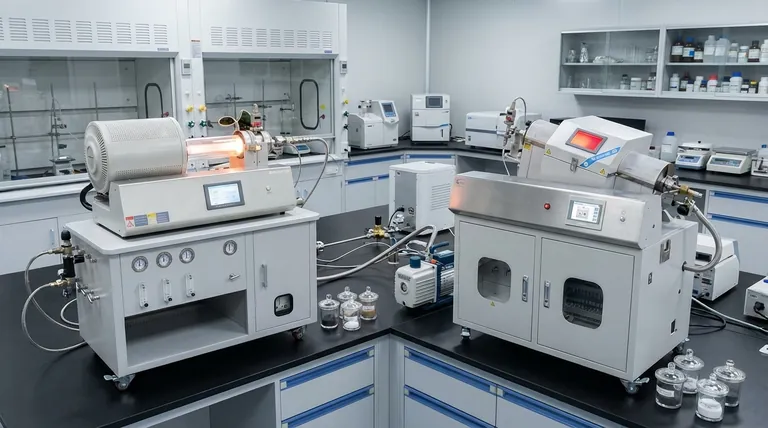
Visual Guide
Related Products
- HFCVD Machine System Equipment for Drawing Die Nano Diamond Coating
- 915MHz MPCVD Diamond Machine Microwave Plasma Chemical Vapor Deposition System Reactor
- RF PECVD System Radio Frequency Plasma Enhanced Chemical Vapor Deposition
- Custom Made Versatile CVD Tube Furnace Chemical Vapor Deposition CVD Equipment Machine
- Slide PECVD Tube Furnace with Liquid Gasifier PECVD Machine
People Also Ask
- How can customers maximize the quality of CVD coatings? Master Pre-Coating Prep for Superior Results
- What are the equipment for chemical vapor deposition? A Guide to the 5 Essential Components
- What core function does CVD equipment serve in h-BN anti-corrosion? Master Precision Synthesis for High-Performance Films
- What materials are commonly used in CVD coating systems? Explore Key Materials for Superior Coatings
- What is the advantage of using a CVD system for coating turbine blades? Master Complex Geometries with Ease


