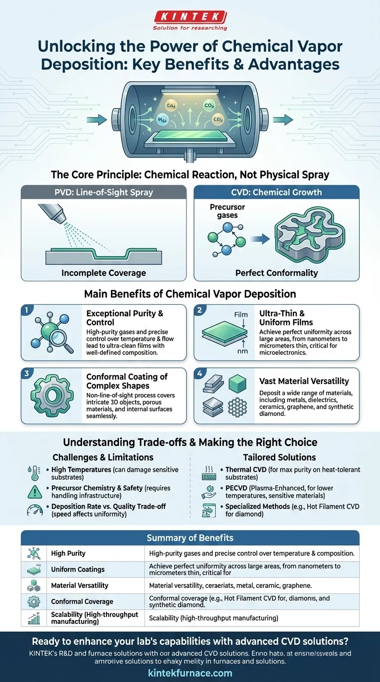
At its core, Chemical Vapor Deposition (CVD) offers a combination of material versatility, film quality, and geometric flexibility that is difficult to achieve with other methods. Its primary benefits include the ability to create highly pure and uniform coatings, deposit a vast range of materials, and perfectly cover complex, non-line-of-sight surfaces.
The true advantage of CVD lies in its fundamental nature: it is a chemical process, not a physical one. This allows it to "grow" a film atom-by-atom on every exposed surface, resulting in exceptionally uniform and pure layers that are impossible to create with directional, line-of-sight deposition techniques.
The Core Principle: Why CVD Excels at Film Quality
The unique advantages of CVD stem directly from how it works. A precursor gas is introduced into a chamber where it reacts and decomposes, depositing a solid film onto a substrate.
It's a Chemical Reaction, Not a Physical Spray
Unlike physical vapor deposition (PVD), which essentially sprays material from a source to a target, CVD involves a chemical reaction that occurs across the entire surface of the substrate.
This gas-phase reaction ensures that the depositing material can reach every crack, crevice, and internal feature of an object.
Achieving Exceptional Purity and Control
The inputs to a CVD process are high-purity gases. By precisely managing the flow rates, temperature, and pressure within the reaction chamber, engineers can exert fine-grained control over the final film.
This allows for the creation of films with extremely high material purity and a well-defined composition and microstructure.
Creating Ultra-Thin and Uniform Films
CVD is capable of producing films that are perfectly uniform across large areas. The process can be controlled to deposit layers from just a few atoms thick (nanometers) up to many micrometers.
This precision is fundamental to modern industries like microelectronics, where the performance of a transistor depends on the quality of unimaginably thin dielectric and conductive layers.
Unmatched Versatility in Materials and Substrates
Beyond film quality, CVD's flexibility makes it a go-to solution for a wide array of engineering challenges.
Coating Complex Shapes: The Power of Conformality
The most significant geometric benefit of CVD is its conformality. Because the process is not line-of-sight, it can deposit a perfectly uniform coating on complex 3D objects, porous materials, and internal surfaces.
This is critical for applications like creating protective barriers against corrosion inside pipes or depositing functional layers on intricate micro-electro-mechanical systems (MEMS).
A Vast Library of Depositable Materials
By changing the precursor gases and process conditions, CVD can be used to deposit an enormous range of materials.
This includes metals, conductive films, dielectric layers, ceramics, and advanced materials like graphene and synthetic diamond. This versatility is unmatched by most other deposition techniques.
Scalability for Industrial Production
While the equipment can be complex, CVD processes are highly scalable. They are used in high-throughput manufacturing for everything from solar panels and flat-panel displays to protective coatings on cutting tools.
Once a process is dialed in, it can be reliably replicated across large-area substrates or large batches of parts, making it cost-effective at an industrial scale.
Understanding the Trade-offs and Limitations
No process is without its challenges. Objectively understanding the limitations of CVD is key to using it effectively.
The Challenge of High Temperatures
Traditional CVD processes often require very high temperatures (several hundred to over a thousand degrees Celsius) to drive the necessary chemical reactions.
This can damage or destroy temperature-sensitive substrates, such as plastics or certain electronic components.
Precursor Chemistry and Safety
The gases used in CVD can be toxic, flammable, or corrosive, requiring significant investment in safety and handling infrastructure.
Furthermore, unwanted chemical byproducts can form during the reaction, which must be managed and safely disposed of.
Deposition Rate vs. Film Quality
While CVD can have high deposition rates, there is often a trade-off. Attempting to deposit a film too quickly can compromise its uniformity, density, and purity.
Achieving the highest quality films often requires slower, more carefully controlled deposition conditions.
Making the Right Choice for Your Goal
The specific type of CVD process you choose depends entirely on your material, substrate, and desired outcome.
- If your primary focus is maximum purity and conformality on a heat-tolerant substrate: Traditional thermal CVD is the ideal choice for creating dense, high-quality films.
- If your primary focus is coating a temperature-sensitive material like a polymer or a completed electronic device: Plasma-Enhanced CVD (PECVD) is the solution, as it uses plasma to enable reactions at much lower temperatures.
- If your primary focus is creating ultra-hard, high-performance coatings for tools or optics: Specialized methods like Hot Filament CVD (for diamond films) are specifically designed for these demanding applications.
Ultimately, Chemical Vapor Deposition is a foundational technology that empowers engineers to build materials and devices from the atom up.
Summary Table:
| Benefit | Description |
|---|---|
| High Purity | Uses pure gases for clean, controlled film deposition with minimal impurities. |
| Uniform Coatings | Ensures even film thickness across surfaces, ideal for complex geometries. |
| Material Versatility | Deposits metals, ceramics, graphene, and more by changing precursor gases. |
| Conformal Coverage | Covers non-line-of-sight areas, perfect for intricate parts and internal surfaces. |
| Scalability | Easily adapted for industrial production, supporting high-throughput manufacturing. |
Ready to enhance your lab's capabilities with advanced CVD solutions? At KINTEK, we leverage exceptional R&D and in-house manufacturing to provide high-temperature furnace solutions tailored for diverse laboratories. Our product line includes Muffle, Tube, Rotary Furnaces, Vacuum & Atmosphere Furnaces, and CVD/PECVD Systems, all backed by strong deep customization to meet your unique experimental needs. Contact us today to discuss how our expertise can help you achieve superior film deposition and optimize your processes!
Visual Guide
Related Products
- Custom Made Versatile CVD Tube Furnace Chemical Vapor Deposition CVD Equipment Machine
- RF PECVD System Radio Frequency Plasma Enhanced Chemical Vapor Deposition
- MPCVD Machine System Reactor Bell-jar Resonator for Lab and Diamond Growth
- 915MHz MPCVD Diamond Machine Microwave Plasma Chemical Vapor Deposition System Reactor
- Slide PECVD Tube Furnace with Liquid Gasifier PECVD Machine
People Also Ask
- How does CVD tube furnace sintering enhance graphene growth? Achieve Superior Crystallinity and High Electron Mobility
- What temperature range do standard CVD tube furnaces operate at? Unlock Precision for Your Material Deposition
- What is a CVD tube furnace and what is its primary function? Discover Precision Thin-Film Deposition
- What future trends are expected in the development of CVD tube furnaces? Discover Smarter, More Versatile Systems
- What are the key features of CVD tube furnaces for 2D material processing? Unlock Precision Synthesis for Superior Materials


