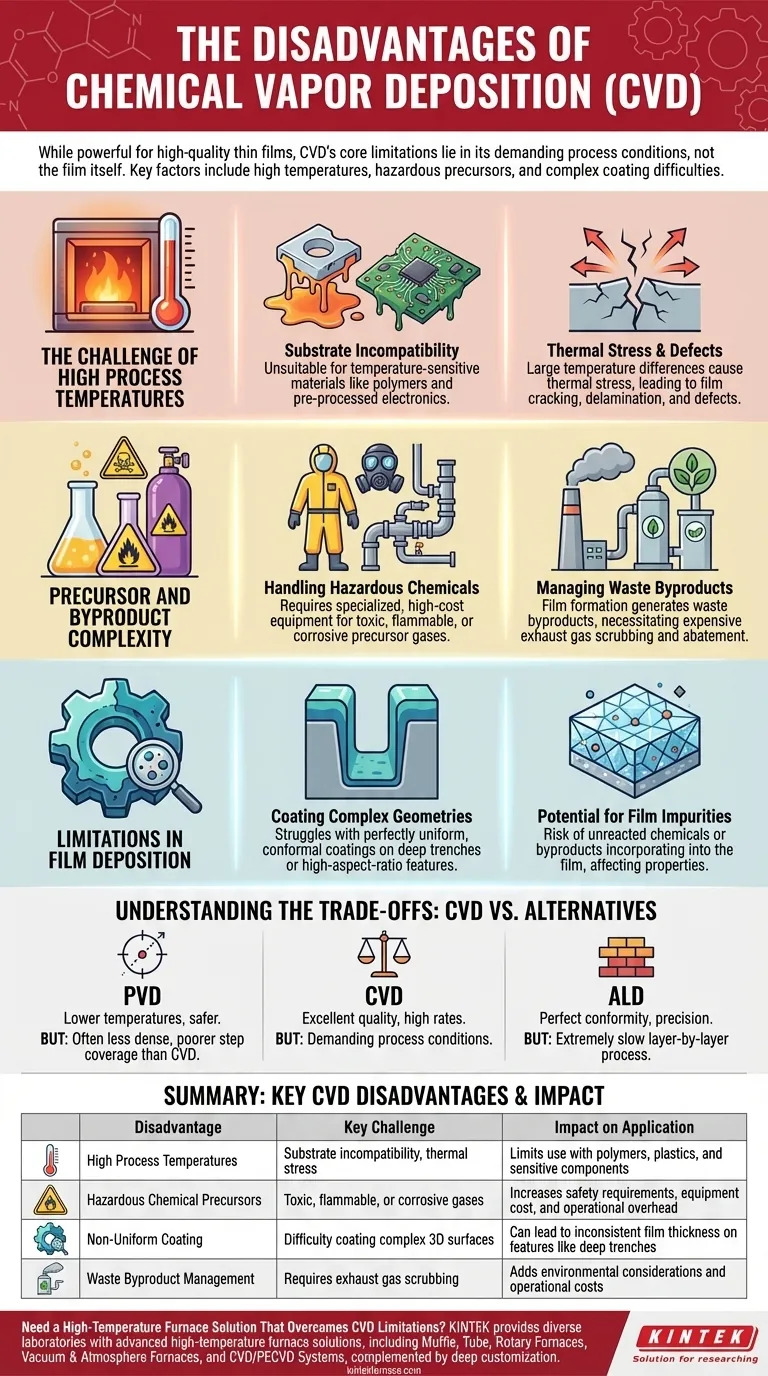
While a powerful technique for creating high-quality thin films, the primary disadvantages of Chemical Vapor Deposition (CVD) are its reliance on high process temperatures, the use of often hazardous chemical precursors, and its difficulty in uniformly coating complex three-dimensional surfaces. These factors can limit the types of materials you can use as a substrate and add significant operational complexity and cost.
Chemical Vapor Deposition offers excellent film quality and high deposition rates, but its core limitations are not in the film itself, but in the demanding process conditions required to create it. The key is to determine if your substrate and application can tolerate the heat and chemical environment.
The Challenge of High Process Temperatures
One of the most significant constraints of many CVD processes is the heat required to initiate the chemical reactions.
Substrate Incompatibility
The high temperatures, often several hundred degrees Celsius, make CVD unsuitable for temperature-sensitive substrates. Materials like polymers, plastics, or certain pre-processed electronic components can be damaged, melted, or degraded by the heat.
Thermal Stress and Defects
A large temperature difference between the hot deposition process and room temperature can create significant thermal stress. This occurs due to mismatched thermal expansion coefficients between the deposited film and the substrate, potentially leading to film cracking, delamination, or defects.
Precursor and Byproduct Complexity
CVD is fundamentally a chemical process, which introduces challenges related to the materials used and the waste generated.
Handling Hazardous Chemicals
The precursor gases used in CVD are often toxic, flammable, or corrosive. This necessitates specialized, high-cost equipment for gas delivery, safety monitoring, and operator protection, increasing both capital investment and operational overhead.
Managing Waste Byproducts
The chemical reactions that form the film also produce unwanted byproducts. These waste gases must be properly managed and scrubbed from the exhaust stream, which requires additional abatement equipment and adds environmental and financial costs to the process.
Limitations in Film Deposition
While CVD creates durable films, achieving perfect coverage and purity is not always straightforward.
Coating Complex Geometries
CVD can struggle to deposit a perfectly uniform, or conformal, film over substrates with complex topographies, such as deep trenches or high-aspect-ratio features. The gas-phase reaction dynamics can lead to thicker deposits at the opening of a feature and thinner, incomplete coverage at the bottom.
Potential for Film Impurities
Because the reaction occurs on the surface from gaseous precursors, there is a risk that unreacted chemicals or byproducts can become incorporated into the growing film. These impurities can negatively affect the film's electrical, optical, or mechanical properties.
Understanding the Trade-offs: CVD vs. Alternatives
No deposition method is perfect. The disadvantages of CVD are best understood in the context of its primary alternatives.
The CVD vs. PVD Compromise
Physical Vapor Deposition (PVD) is a line-of-sight process that typically operates at lower temperatures and does not use the same hazardous chemical precursors. However, CVD films are often denser, more crystalline, and have superior adhesion and step coverage compared to PVD films.
The Speed vs. Precision Dilemma
Atomic Layer Deposition (ALD), a subset of CVD, offers unparalleled control and can create perfectly conformal coatings on the most complex shapes. The trade-off is speed; ALD is an extremely slow, layer-by-layer process, whereas CVD can deposit films much more quickly, making it better for thicker coatings and high-throughput manufacturing.
Making the Right Choice for Your Application
Selecting a deposition technology requires matching the process capabilities to your end goal.
- If your primary focus is coating heat-sensitive materials or avoiding complex chemical handling: You should strongly consider alternatives like PVD or sputtering.
- If your primary focus is achieving perfect uniformity on extremely complex 3D structures: Atomic Layer Deposition (ALD) is often the superior choice, provided you can accept its slower deposition rate.
- If your primary focus is producing high-quality, durable, and dense films on robust substrates at high speeds: CVD remains an excellent and industry-standard method if you can manage its process requirements.
By understanding these fundamental limitations, you can confidently select a deposition technology that aligns process realities with your specific material and performance goals.
Summary Table:
| Disadvantage | Key Challenge | Impact on Application |
|---|---|---|
| High Process Temperatures | Substrate incompatibility, thermal stress | Limits use with polymers, plastics, and sensitive components |
| Hazardous Chemical Precursors | Toxic, flammable, or corrosive gases | Increases safety requirements, equipment cost, and operational overhead |
| Non-Uniform Coating | Difficulty coating complex 3D surfaces | Can lead to inconsistent film thickness on features like deep trenches |
| Waste Byproduct Management | Requires exhaust gas scrubbing | Adds environmental considerations and operational costs |
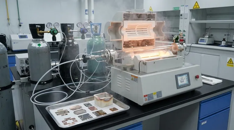
Need a High-Temperature Furnace Solution That Overcomes CVD Limitations?
Leveraging exceptional R&D and in-house manufacturing, KINTEK provides diverse laboratories with advanced high-temperature furnace solutions. Our product line, including Muffle, Tube, Rotary Furnaces, Vacuum & Atmosphere Furnaces, and CVD/PECVD Systems, is complemented by our strong deep customization capability to precisely meet unique experimental requirements.
Let us help you select or customize the right equipment for your specific deposition challenges. Contact our experts today to discuss your application and discover how our solutions can enhance your lab's efficiency and safety.
Visual Guide
Related Products
- Custom Made Versatile CVD Tube Furnace Chemical Vapor Deposition CVD Equipment Machine
- RF PECVD System Radio Frequency Plasma Enhanced Chemical Vapor Deposition
- MPCVD Machine System Reactor Bell-jar Resonator for Lab and Diamond Growth
- 915MHz MPCVD Diamond Machine Microwave Plasma Chemical Vapor Deposition System Reactor
- Slide PECVD Tube Furnace with Liquid Gasifier PECVD Machine
People Also Ask
- What are the benefits of developing new precursor materials for CVD tube furnaces? Unlock Advanced Thin-Film Synthesis
- Which industries and research fields benefit from CVD tube furnace sintering systems for 2D materials? Unlock Next-Gen Tech Innovations
- What future trends are expected in the development of CVD tube furnaces? Discover Smarter, More Versatile Systems
- How can integrating CVD tube furnaces with other technologies benefit device fabrication? Unlock Advanced Hybrid Processes
- What temperature range do standard CVD tube furnaces operate at? Unlock Precision for Your Material Deposition


