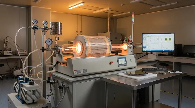
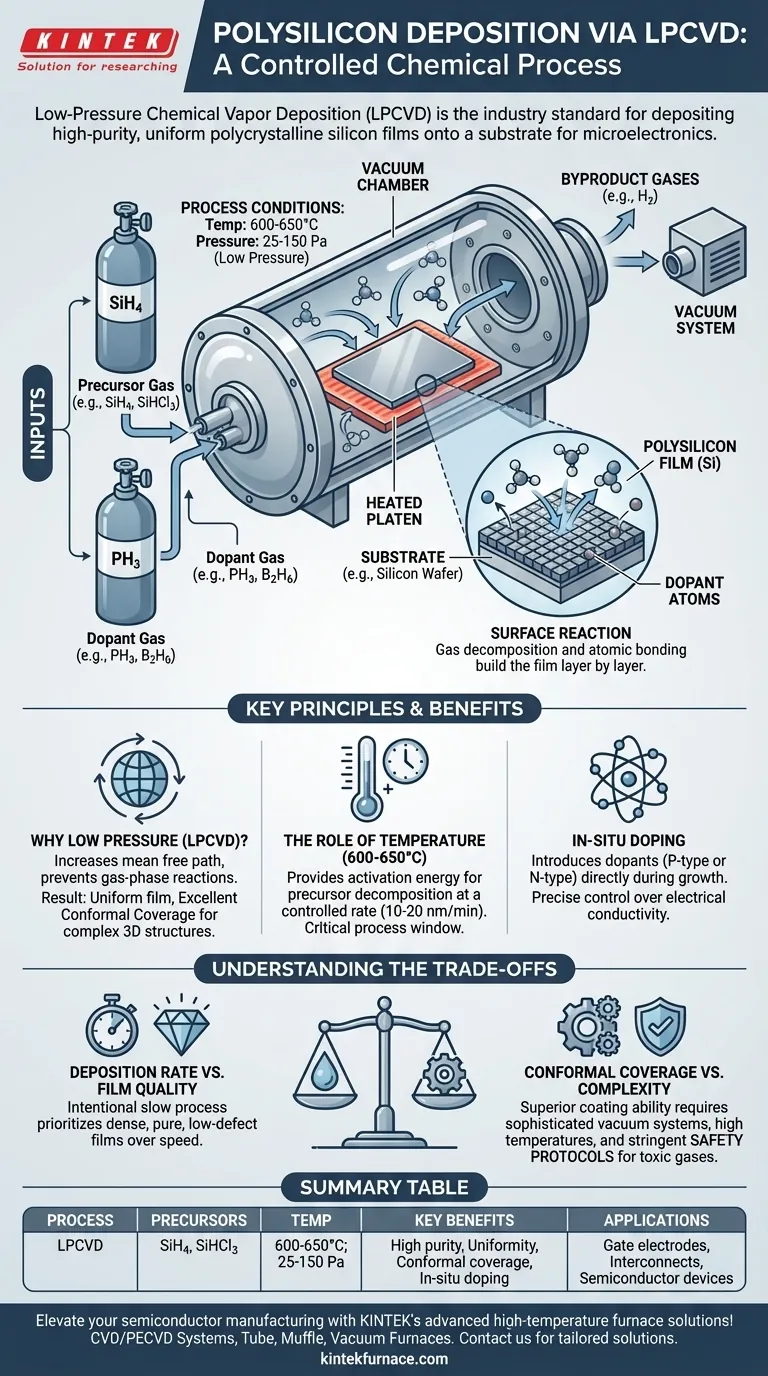
To deposit polysilicon, engineers use a specific method called Low-Pressure Chemical Vapor Deposition (LPCVD). In this process, a precursor gas like silane (SiH4) or trichlorosilane (SiHCl3) is introduced into a vacuum chamber containing the substrate. The chamber is heated to between 600-650°C at a low pressure of 25-150 Pa, causing the gas to decompose and deposit a thin, uniform film of high-purity polycrystalline silicon onto the substrate surface.
The key to understanding polysilicon deposition is to see it not as a simple coating process, but as a controlled chemical reaction on a surface. The precise control of temperature, pressure, and gas chemistry allows for the construction of a highly uniform and pure silicon film, which is the foundational requirement for modern microelectronics.
The Fundamental Principles of CVD
Chemical Vapor Deposition (CVD) is a process designed to build a solid material from a gas. It involves placing a substrate, or the object to be coated, inside a reaction chamber and introducing a reactive precursor gas.
The Core Components
The process relies on four key elements: a substrate (the foundation), a precursor gas (the building blocks), a vacuum chamber (the controlled environment), and energy, typically heat (the catalyst for the reaction). The precursor gas contains the atoms of the material you wish to deposit.
The Chemical Reaction at the Surface
In thermal CVD, the substrate is heated to a precise temperature. This heat provides the activation energy needed for the precursor gas molecules to break apart, or "decompose," when they come into contact with the hot surface.
The desired atoms—in this case, silicon—then bond to the substrate, building the film layer by layer. All other byproduct molecules from the reaction are removed from the chamber by the vacuum system.
The Specifics of Polysilicon Deposition
While CVD is a general technique, depositing device-quality polysilicon requires a very specific set of conditions, achieved through a method known as LPCVD.
Why Low Pressure (LPCVD) is Critical
Operating at low pressure (25-150 Pa) significantly increases the "mean free path" of the gas molecules, meaning they travel further before colliding with each other. This prevents the gas from reacting in mid-air and instead promotes reactions directly on the substrate surface.
The result is a highly uniform film that provides excellent conformal coverage, meaning it can evenly coat intricate, three-dimensional microstructures on a wafer.
Choosing the Precursor: Silane or Trichlorosilane
The most common precursor gases for polysilicon deposition are silane (SiH4) and trichlorosilane (SiHCl3). When heated, silane decomposes into solid silicon and hydrogen gas (SiH4 → Si + 2H2). The choice of precursor affects the deposition rate and the final properties of the film.
The Role of Temperature
The temperature range of 600-650°C is a critical process window. It is hot enough to provide the energy needed to break the chemical bonds in the precursor gas at a controlled rate, typically yielding a growth of 10-20 nanometers per minute.
If the temperature is too low, the reaction rate becomes impractically slow. If it's too high, the film quality can degrade due to unwanted reactions in the gas phase.
In-Situ Doping for Conductivity
One of the most powerful features of the CVD process is the ability to perform in-situ doping. By adding small amounts of other gases like phosphine (PH3) for n-type doping or diborane (B2H6) for p-type doping, dopant atoms are directly incorporated into the silicon film as it grows.
This technique allows for precise control over the polysilicon's final electrical conductivity, building the desired properties directly into the material from the start.
Understanding the Trade-offs
The LPCVD process for polysilicon is optimized for quality, but this involves inherent trade-offs that are important to understand.
Deposition Rate vs. Film Quality
The process is intentionally slow. The low pressures and controlled temperatures prioritize creating a dense, uniform, and pure film with minimal defects. Any attempt to significantly increase the deposition rate by raising pressure or temperature would compromise the film's quality, making it unsuitable for high-performance electronic devices.
Conformal Coverage vs. Process Complexity
LPCVD provides superior conformal coating, which is essential for modern semiconductor manufacturing. However, this capability comes at the cost of process complexity. The need for vacuum systems, high-temperature furnaces, and the careful handling of precursor gases makes CVD equipment more sophisticated than some alternative deposition methods.
Safety and Gas Handling
The precursor and doping gases used in polysilicon deposition (silane, phosphine, diborane) are highly toxic, flammable, or pyrophoric (igniting spontaneously in air). Managing these materials requires stringent safety protocols, specialized equipment, and significant facility investment.
Making the Right Choice for Your Goal
Your application determines which aspects of the CVD process are most critical.
- If your primary focus is creating high-quality gate electrodes or interconnects: The precision of LPCVD using silane at 600-650°C is the industry standard for achieving the required purity and uniformity.
- If your primary focus is controlling electrical properties from the start: Utilize in-situ doping with phosphine or diborane during the LPCVD process to embed dopants directly into the film's crystal structure.
- If your primary focus is achieving uniform coverage across complex 3D structures: The low-pressure nature of LPCVD is non-negotiable, as its ability to produce a highly conformal film is unmatched for these applications.
By understanding these principles, you can appreciate that polysilicon deposition is a foundational process for intentionally engineering advanced semiconductor materials.
Summary Table:
| Aspect | Details |
|---|---|
| Process | Low-Pressure Chemical Vapor Deposition (LPCVD) |
| Precursor Gases | Silane (SiH4) or Trichlorosilane (SiHCl3) |
| Temperature Range | 600-650°C |
| Pressure Range | 25-150 Pa |
| Key Benefits | High purity, uniform film, conformal coverage, in-situ doping capability |
| Applications | Gate electrodes, interconnects, semiconductor devices |
Elevate your semiconductor manufacturing with KINTEK's advanced high-temperature furnace solutions! Leveraging exceptional R&D and in-house manufacturing, we provide diverse laboratories with reliable systems like Muffle, Tube, Rotary, Vacuum & Atmosphere Furnaces, and CVD/PECVD Systems. Our strong deep customization capability ensures precise alignment with your unique experimental needs, from polysilicon deposition to complex material processing. Contact us today to discuss how our tailored solutions can optimize your processes and drive innovation in your projects!
Visual Guide
Related Products
- 915MHz MPCVD Diamond Machine Microwave Plasma Chemical Vapor Deposition System Reactor
- RF PECVD System Radio Frequency Plasma Enhanced Chemical Vapor Deposition
- MPCVD Machine System Reactor Bell-jar Resonator for Lab and Diamond Growth
- HFCVD Machine System Equipment for Drawing Die Nano Diamond Coating
- Custom Made Versatile CVD Tube Furnace Chemical Vapor Deposition CVD Equipment Machine
People Also Ask
- What is the basic principle of operation for the microwave plasma chemical vapor deposition system? Unlock High-Purity Material Growth
- What are some key features and benefits of the microwave plasma chemical vapor deposition system? Achieve Unmatched Material Synthesis
- What are the essential components of an MPCVD reactor system? Build a Pristine Environment for High-Purity Materials
- What are the main components of an MPCVD machine? Unlock the Secrets of Diamond Synthesis
- How does the MPCVD process work to deposit diamond? A Guide to High-Purity Synthesis


