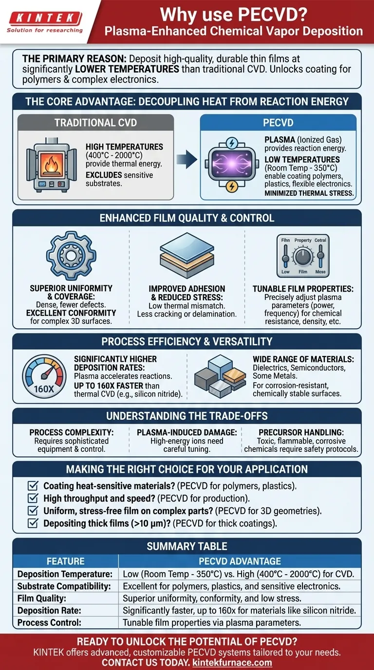
The primary reason to use PECVD is its ability to deposit high-quality, durable thin films at significantly lower temperatures than traditional Chemical Vapor Deposition (CVD). This single advantage unlocks the ability to coat temperature-sensitive materials, such as polymers and complex electronics, that would be damaged or destroyed by high-heat processes.
PECVD is not just a low-temperature version of CVD; it is a fundamentally different approach. By using plasma to provide the reaction energy instead of heat, it offers greater control over film properties, achieves faster deposition rates, and enables the coating of materials that were previously incompatible with vapor deposition techniques.
The Core Advantage: Decoupling Heat from Reaction Energy
How Traditional CVD Works
Conventional CVD relies on high temperatures, often between 400°C and 2000°C, to provide the thermal energy needed to break down precursor gases and initiate the chemical reactions that form a film on a substrate.
This extreme heat is the primary limiting factor, as it excludes any substrate that cannot withstand such temperatures.
How PECVD Changes the Equation
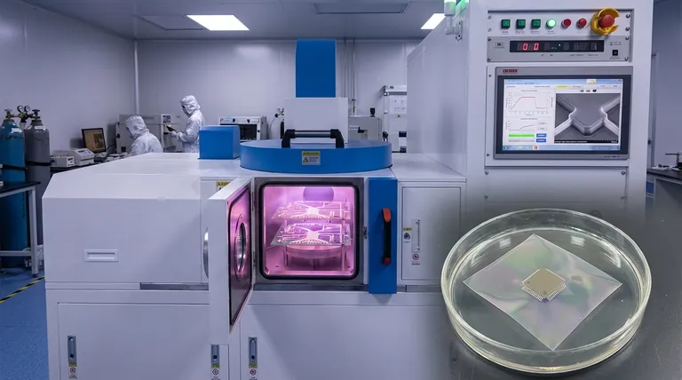
Plasma-Enhanced Chemical Vapor Deposition (PECVD) introduces energy into the system using an electric field to create plasma, an ionized gas.
This plasma, not intense heat, provides the energy to activate the precursor gases and drive the chemical reactions. This allows the deposition process to occur at much lower temperatures, from room temperature up to around 350°C.
The Impact: Low-Temperature Deposition
By removing the dependency on high heat, PECVD makes it possible to apply high-performance coatings to a vast new range of materials.
This includes polymers, plastics, flexible electronics, and fully assembled devices that contain sensitive components. The lower temperature also dramatically reduces thermal stress in the deposited film.
Enhanced Film Quality and Control
Superior Film Uniformity and Coverage
The plasma-driven process promotes the creation of dense, high-quality films with fewer pinholes or defects compared to other methods.
PECVD is renowned for its excellent conformity, meaning it can evenly coat complex, three-dimensional surfaces and fill intricate micro-features without voids. This is often a significant advantage over line-of-sight processes like Physical Vapor Deposition (PVD).
Improved Adhesion and Reduced Stress
Depositing a film at high temperatures onto a cooler substrate creates significant thermal stress as the materials cool at different rates, often leading to cracking or poor adhesion.
Because PECVD operates at low temperatures, the thermal mismatch between the film and the substrate is minimized. This results in low-stress films that exhibit superior bonding and are far less likely to crack or delaminate.
Tunable Film Properties
In a PECVD system, film characteristics are not just a function of temperature and gas flow. Operators can precisely adjust plasma parameters like power and frequency.
This additional control allows for the fine-tuning of the film's final properties, such as its chemical resistance, density, electrical performance, and even its polymer-like characteristics.
Process Efficiency and Versatility
Significantly Higher Deposition Rates
The plasma environment dramatically accelerates the chemical reactions involved in deposition.
For certain materials, like silicon nitride, PECVD can achieve deposition rates that are over 160 times faster than conventional thermal CVD. This high throughput is a critical advantage in manufacturing environments.
Wide Range of Materials
PECVD is an incredibly versatile technique capable of depositing a broad spectrum of materials.
This includes critical industrial materials like dielectrics (silicon dioxide, silicon nitride), semiconductors (amorphous silicon), and even some metals, often used to create corrosion-resistant or chemically stable surfaces.
Understanding the Trade-offs
Process Complexity
While powerful, PECVD is more complex than a simple thermal CVD system. Managing the plasma generation, gas chemistry, and vacuum conditions requires more sophisticated equipment and process control.
Potential for Plasma-Induced Damage
The high-energy ions within the plasma can, if not properly controlled, cause damage to the surface of extremely sensitive substrates. Careful tuning of the process parameters is required to mitigate this risk.
Precursor Handling
Like all CVD processes, PECVD relies on chemical precursors that can be toxic, flammable, or corrosive. Proper engineering controls and safety protocols are essential for handling these materials.
Making the Right Choice for Your Application
Choosing a deposition method requires aligning the process capabilities with your primary goal.
- If your primary focus is coating heat-sensitive materials: PECVD is the clear and often only choice for applying high-quality coatings to polymers, plastics, or pre-fabricated devices.
- If your primary focus is high throughput and speed: PECVD's exceptionally high deposition rates for materials like silicon nitride make it ideal for production-scale manufacturing.
- If your primary focus is creating a uniform, stress-free film on complex parts: PECVD's excellent conformity and low-stress properties are superior for coating intricate 3D geometries.
- If your primary focus is depositing thick films (greater than 10 μm): PECVD has a unique capability for building up thick coatings that are not typically achievable with conventional CVD.
By leveraging plasma instead of heat, PECVD fundamentally expands the possibilities of what materials can be made and what surfaces can be engineered.
Summary Table:
| Feature | PECVD Advantage |
|---|---|
| Deposition Temperature | Low (Room Temp - 350°C) vs. High (400°C - 2000°C) for CVD |
| Substrate Compatibility | Excellent for polymers, plastics, and sensitive electronics |
| Film Quality | Superior uniformity, conformity, and low stress |
| Deposition Rate | Significantly faster, up to 160x for materials like silicon nitride |
| Process Control | Tunable film properties via plasma parameters |
Ready to unlock the potential of PECVD for your lab?
At KINTEK, we leverage our exceptional R&D and in-house manufacturing to provide advanced PECVD systems tailored to your unique needs. Whether you're working with temperature-sensitive polymers, complex 3D parts, or require high-throughput production, our deep customization capabilities ensure a perfect fit for your experimental requirements.
Contact us today to discuss how our PECVD solutions can enhance your thin film deposition process and drive your research forward. Get in touch via our contact form!
Visual Guide
Related Products
- Slide PECVD Tube Furnace with Liquid Gasifier PECVD Machine
- RF PECVD System Radio Frequency Plasma Enhanced Chemical Vapor Deposition
- Inclined Rotary Plasma Enhanced Chemical Deposition PECVD Tube Furnace Machine
- Inclined Rotary Plasma Enhanced Chemical Deposition PECVD Tube Furnace Machine
- Multi Heating Zones CVD Tube Furnace Machine for Chemical Vapor Deposition Equipment
People Also Ask
- How does PECVD equipment contribute to TOPCon bottom cells? Mastering Hydrogenation for Maximum Solar Efficiency
- How does a hydrogen reduction environment in an industrial tube furnace facilitate gold-copper alloy microspheres?
- In which industries is the tube furnace commonly used? Essential for Materials Science, Energy, and More
- What are the disadvantages of tube furnace cracking when processing heavy raw materials? Avoid Costly Downtime and Inefficiency
- What are the typical conditions for plasma-enhanced CVD processes? Achieve Low-Temperature Thin Film Deposition


