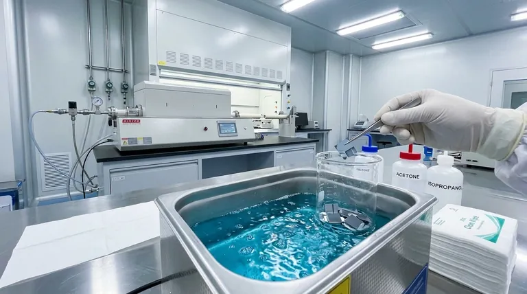
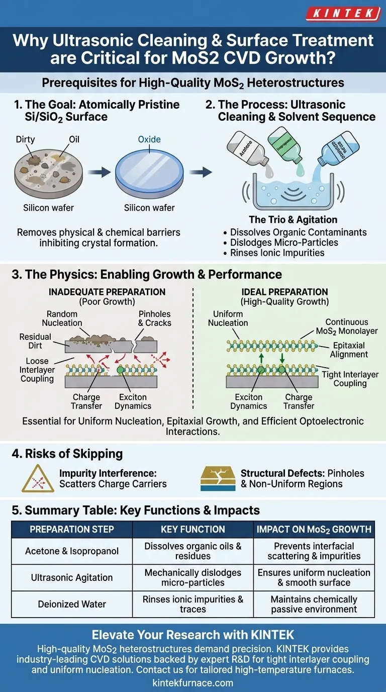
Ultrasonic cleaning and surface treatment are critical prerequisites for Chemical Vapor Deposition (CVD) because they eliminate the physical and chemical barriers that inhibit high-quality crystal formation. By utilizing a specific sequence of deionized water, acetone, and isopropanol, you create an ultra-clean Si/SiO2 surface necessary for the uniform nucleation and epitaxial growth of Molybdenum Disulfide (MoS2) monolayers.
A pristine substrate is the foundation of a functional heterostructure. Without thorough cleaning, contaminants disrupt the atomic interface, preventing the tight interlayer coupling required for efficient exciton dynamics and charge transfer.
Achieving an Atomically Pristine Surface
The Solvent Sequence
The cleaning process typically involves a specific trio of solvents: acetone, isopropanol, and deionized water.
Acetone and isopropanol are essential for dissolving and lifting organic contaminants such as oils or resist residues left from previous processing steps.
Deionized water is used to rinse away any remaining solvent traces and ionic impurities.
The Role of Ultrasonication
Simply soaking the substrate is often insufficient to dislodge stubborn debris.
Ultrasonic agitation provides the mechanical energy needed to detach micro-particles from the substrate surface.
This ensures that the surface is physically smooth and chemically passive before entering the CVD furnace.
The Physics of Growth and Performance
Facilitating Nucleation and Epitaxy
For MoS2 to grow in a single, continuous atomic layer, it requires a uniform surface energy profile.
A clean surface allows for controlled nucleation, where the atomic growth begins at specific, desired points rather than randomly on dirt particles.
Furthermore, removing contaminants facilitates epitaxial growth, allowing the MoS2 lattice to align correctly relative to the substrate or underlying layers.
Optimizing Electronic Properties
The performance of a heterostructure depends heavily on how well the layers interact with each other.
A residue-free interface ensures tight interlayer coupling, which is the physical proximity required for layers to "talk" to one another electronically.
This coupling is vital for preserving intrinsic exciton dynamics (the behavior of electron-hole pairs) and facilitating efficient charge transfer between layers.
Risks of Inadequate Preparation
Impurity Interference
If the cleaning step is skipped or performed poorly, residual impurities become embedded in the interface.
These impurities act as scattering centers, interfering with the movement of charge carriers.
Structural Defects
Contaminants can physically block the flow of precursor gases during CVD.
This results in pinholes, cracks, or non-uniform regions in the MoS2 monolayer, rendering the material unsuitable for high-precision device applications.
Maximizing CVD Success
To ensure your MoS2 heterostructures perform as intended, align your cleaning protocol with your specific experimental goals:
- If your primary focus is Crystal Quality: rigorous removal of micro-particles is required to prevent physical defects and ensure uniform nucleation and epitaxial growth.
- If your primary focus is Optoelectronic Performance: rigorous removal of organic contaminants is required to ensure tight interlayer coupling and prevent interference with exciton dynamics.
The success of your CVD process is determined before the furnace is even turned on; it begins with the purity of your substrate.
Summary Table:
| Preparation Step | Key Function | Impact on MoS2 Growth |
|---|---|---|
| Acetone & Isopropanol | Dissolves organic oils and resist residues | Prevents interfacial scattering & impurities |
| Ultrasonic Agitation | Mechanically dislodges micro-particles | Ensures uniform nucleation and smooth surface |
| Deionized Water | Rinses ionic impurities and solvent traces | Maintains a chemically passive environment |
| Surface Treatment | Normalizes surface energy | Facilitates epitaxial alignment & layer coupling |
Elevate Your Material Research with KINTEK
High-quality MoS2 heterostructures demand precision at every stage—from substrate preparation to the final growth cycle. KINTEK provides the industry-leading laboratory solutions required for sophisticated CVD, CVD, and Vacuum systems. Our equipment is backed by expert R&D and manufacturing, ensuring you achieve the tight interlayer coupling and uniform nucleation necessary for next-generation optoelectronics.
Whether you need standard or fully customizable high-temperature furnaces for your unique research needs, we are here to support your success.
Ready to optimize your thin-film growth? Contact KINTEK today for expert guidance and tailored solutions!
Visual Guide
References
- Vaibhav Varade, Jana Vejpravová. Sulfur isotope engineering in heterostructures of transition metal dichalcogenides. DOI: 10.1039/d4na00897a
This article is also based on technical information from Kintek Furnace Knowledge Base .
Related Products
- HFCVD Machine System Equipment for Drawing Die Nano Diamond Coating
- Cylindrical Resonator MPCVD Machine System for Lab Diamond Growth
- Custom Made Versatile CVD Tube Furnace Chemical Vapor Deposition CVD Equipment Machine
- 915MHz MPCVD Diamond Machine Microwave Plasma Chemical Vapor Deposition System Reactor
- MPCVD Machine System Reactor Bell-jar Resonator for Lab and Diamond Growth
People Also Ask
- What is chemical vapor deposition (CVD) and its primary industrial application? Unlock Precision Thin Films for Electronics
- How can customers maximize the quality of CVD coatings? Master Pre-Coating Prep for Superior Results
- What is the function of high-purity Argon (Ar) gas during CVD? Optimize Your Thin Film Uniformity and Purity
- What role does Chemical Vapor Deposition (CVD) equipment play in the surface coating of carbon fibers for composites?
- What materials are commonly used in CVD coating systems? Explore Key Materials for Superior Coatings