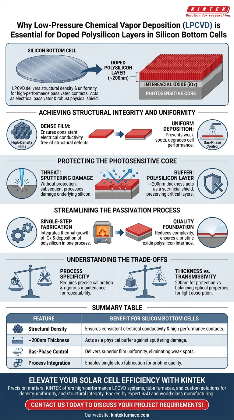
LPCVD equipment is essential for creating the doped polysilicon layers in silicon bottom cells because it delivers the structural density and uniformity required for high-performance passivated contacts. Specifically, it deposits a layer roughly 200 nanometers thick that serves a dual purpose: facilitating electrical passivation and acting as a robust physical shield against damage during later manufacturing steps.
LPCVD provides the precision necessary to deposit a dense, uniform polysilicon film that functions as an integral part of the cell's passivated contact. Crucially, the substantial thickness of this layer protects sensitive underlying structures from sputtering damage, ensuring the cell maintains optimal electrical performance.
Achieving Structural Integrity and Uniformity
The Necessity of High-Density Films
For a passivated contact to function correctly, the polysilicon layer must be free of structural defects. LPCVD creates a highly dense film that ensures consistent electrical conductivity. This density is critical for the overall efficiency of the contact layer.
Precision Through Gas-Phase Control
LPCVD systems operate by strictly controlling chemical reactions in the gas phase. This precision results in a uniform deposition across the silicon wafer surface. Such uniformity prevents weak spots that could degrade the cell's performance.
Protecting the Photosensitive Core
The Threat of Sputtering Damage
Subsequent processing steps in solar cell manufacturing often involve sputtering, a high-energy process used to apply other materials. Without protection, this process can physically damage the underlying photosensitive silicon layers. Such damage compromises the electrical performance of the bottom cell.
The Polysilicon Layer as a Buffer
The doped polysilicon layer deposited by LPCVD is specifically engineered to be approximately 200 nanometers thick. This "substantial" thickness acts as a sacrificial buffer or shield. It absorbs the impact of subsequent processing, preserving the integrity of the critical layers beneath it.
Streamlining the Passivation Process
Enabling Single-Step Fabrication
Advanced horizontal tube LPCVD systems can integrate multiple formation steps. They enable the thermal growth of the interfacial oxide (iOx) layer and the deposition of the polysilicon layer in a single process.
Building a Foundation for Quality
By combining these steps, the equipment establishes a cohesive foundation for high-quality passivation structures. This integration reduces process complexity while ensuring the interface between the oxide and polysilicon is pristine.
Understanding the Trade-offs
Process Specificity
While LPCVD offers superior uniformity, it requires precise calibration of gas-phase reactions. This level of control is demanding and necessitates rigorous equipment maintenance to ensure repeatability.
Thickness vs. Transmissivity
The 200-nanometer thickness is vital for protection, but it introduces a dense material layer to the stack. Manufacturers must balance the need for this protective thickness against the optical properties required for the cell design, ensuring the layer aids conductivity without hindering light absorption where relevant.
Optimizing Silicon Bottom Cell Fabrication
To ensure you are utilizing LPCVD equipment effectively for your specific manufacturing goals, consider the following:
- If your primary focus is process yield: Prioritize the 200nm thickness specification to ensure maximum protection against sputtering damage in downstream steps.
- If your primary focus is passivation quality: Utilize the single-step capability to grow the interfacial oxide and polysilicon simultaneously, minimizing interface contamination.
Ultimately, LPCVD is not just a deposition tool; it is a critical safeguard that preserves the electrical integrity of the entire solar cell stack.
Summary Table:
| Feature | Benefit for Silicon Bottom Cells |
|---|---|
| Structural Density | Ensures consistent electrical conductivity and high-performance passivated contacts. |
| 200nm Thickness | Acts as a physical buffer to protect sensitive layers from subsequent sputtering damage. |
| Gas-Phase Control | Delivers superior film uniformity across the wafer surface, eliminating performance weak spots. |
| Process Integration | Enables single-step fabrication of interfacial oxide (iOx) and polysilicon layers for pristine quality. |
Elevate Your Solar Cell Efficiency with KINTEK
Precision matters when depositing critical polysilicon layers. Backed by expert R&D and world-class manufacturing, KINTEK offers high-performance LPCVD systems, tube furnaces, and customizable high-temp solutions tailored for your unique silicon bottom cell requirements. Our equipment ensures the density, uniformity, and structural integrity your high-efficiency solar projects demand.
Ready to optimize your passivation process? Contact us today to discuss your project requirements!
Visual Guide
References
- Rasmus Nielsen, Peter C. K. Vesborg. Monolithic Selenium/Silicon Tandem Solar Cells. DOI: 10.1103/prxenergy.3.013013
This article is also based on technical information from Kintek Furnace Knowledge Base .
Related Products
- Custom Made Versatile CVD Tube Furnace Chemical Vapor Deposition CVD Equipment Machine
- Multi Heating Zones CVD Tube Furnace Machine for Chemical Vapor Deposition Equipment
- 915MHz MPCVD Diamond Machine Microwave Plasma Chemical Vapor Deposition System Reactor
- HFCVD Machine System Equipment for Drawing Die Nano Diamond Coating
- Slide PECVD Tube Furnace with Liquid Gasifier PECVD Machine
People Also Ask
- What improvements can be made to the bonding force of gate dielectric films using a CVD tube furnace? Enhance Adhesion for Reliable Devices
- What customization options are available for CVD tube furnaces? Tailor Your System for Superior Material Synthesis
- What is a CVD tube furnace and what is its primary function? Discover Precision Thin-Film Deposition
- How might AI and machine learning enhance CVD tube furnace processes? Boost Quality, Speed, and Safety
- What are the key features of CVD tube furnaces for 2D material processing? Unlock Precision Synthesis for Superior Materials


